3D NAND Hits 176 Layers
Micron Technology recently unveiled 176-layer, triple-level-cell (TLC), 3D NAND flash memory with a 30% smaller die size that employs a new replacement-gate (RG) NAND technology. The chips offer a 35% read/write latency improvement as well as a 33% increase in transfer rate, which is now 1600 Mtransfers/s.
The chips are actually built from a pair of 88-layer stacks. When making a 176-layer stack, the challenge is the difficulty in ensuring uniform construction up and down the stack. The latest chips follow on the heels of the 128-layer device from Micron, which also employed 3D NAND and 64-layer stacks.
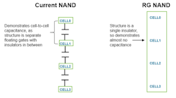
The challenge that RG NAND addresses is the capacitance between cells (Fig. 1). The RG NAND architecture employs a single insulator structure that minimizes the capacitance between cells to almost zero. Each TLC stores three bits of data.
The change to RG NAND improves write endurance and power efficiency while the smaller size boosts overall capacity. Write speed is faster, too, at almost twice that of conventional NAND because the ramp time for programming is reduced by the lower capacitance levels. RG NAND also allows the voltage threshold saturation to be increased so that a cell can hold a larger charge.
With 3D RG NAND, a wider pillar can be built that’s more stable; therefore, more layers can be used in a stack (Fig. 2). The memory stack only contains storage elements as Micron utilizes a CMOS-under-the-array (CUA) approach. This puts the management logic on the bottom layer of the chip with memory layers built on top of it.

About the Author

William G. Wong
Senior Content Director - Electronic Design and Microwaves & RF
I am Editor of Electronic Design focusing on embedded, software, and systems. As Senior Content Director, I also manage Microwaves & RF and I work with a great team of editors to provide engineers, programmers, developers and technical managers with interesting and useful articles and videos on a regular basis. Check out our free newsletters to see the latest content.
You can send press releases for new products for possible coverage on the website. I am also interested in receiving contributed articles for publishing on our website. Use our template and send to me along with a signed release form.
Check out my blog, AltEmbedded on Electronic Design, as well as his latest articles on this site that are listed below.
You can visit my social media via these links:
- AltEmbedded on Electronic Design
- Bill Wong on Facebook
- @AltEmbedded on Twitter
- Bill Wong on LinkedIn
I earned a Bachelor of Electrical Engineering at the Georgia Institute of Technology and a Masters in Computer Science from Rutgers University. I still do a bit of programming using everything from C and C++ to Rust and Ada/SPARK. I do a bit of PHP programming for Drupal websites. I have posted a few Drupal modules.
I still get a hand on software and electronic hardware. Some of this can be found on our Kit Close-Up video series. You can also see me on many of our TechXchange Talk videos. I am interested in a range of projects from robotics to artificial intelligence.
Comment About the Article
To join the conversation, and become an exclusive member of Electronic Design, create an account today!

Leaders relevant to this article: