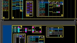
Build a Non-Visible-Connectivity Digital Circuit Simulator with Sliding Data Stack
Download this article in PDF format.
What you'll learn:
- A method for editing a circuit schematic using a GUI, but without having to resort to using lines to define connectivity.
- The steps through the simulation process.
At present, many software tools are available that can assist us in the process of simulating combinational digital circuits. Recent applications use a graphical user interface (GUI) to create schematics using drag-and-drop semantics for placing logic elements. These are then connected by dragging “wires” between elements. Such work is carried out in a non-systematic process that’s not optimal, and changes to the circuit—e.g., deleting or moving elements—isn’t an easy job.
Typically, this type of development also requires another interface to edit simulation vectors. We present an approach that allows a user to continue using a GUI while providing a way to edit the circuit schematic without using lines to define the connectivity between components. Our simulator platform is a Visual Basic 6 application, which can be obtained by email from the author ([email protected]).
General Concepts
The application allows for the definition of a circuit and provides simulation support. Internally, a Reverse Polish Notation-Tovar Algorithmic State Machine (RPN-TASM) algorithm assists in editing of the circuit in the stack.
The TASM algorithm was developed using “Laminar Representation of Finite State Machines.” It’s based on personal interpretations by the author regarding the morphological structure and the writing system of the Maya Codices. Here, all of the states of a sequential machine have the same size and are drawn next to one another. Connectivity between objects within a state and with objects from other states is neither visible nor linear. The idea was to a reduce the language to three instructions.
The system presents a traditional schematic. It also facilitates the creation of simulation vectors and presents behavior graphs of each variable correlated with the behavior of the hardware elements generated by the simulation.
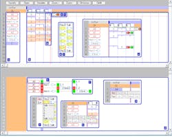
The figure shows the simulator's GUI. The three main blocks are the vertical stack (a), simulation vectors (b), and the traditional schematic presentation (d).
The vertical stack uses RPN and a postfix type mathematical notation to define the circuit. It handles Boolean logic without the graphical connectivity of a typical schematic. The latter is generated by the application based on the stack specification. We did include a bus notation (f).
Editing the Circuit
The application walks the user through the system by starting with a text box on the stack. Objects are selected from a menu and inserted into the stack. As shown in the figure, elements include variables (h) and Boolean functions that present windows with details about the operation (g). The function menu (i) presents the typical schematic images for the Boolean functions. The system steps through definitions of inputs (j) and the final version (k).
Editing the Vectors
The system only allows vector data to be changed for variables in the stack. A popup dialog box lets the user select a 0 or 1 (c). Variable values can be changed by double clicking the variable position in the vector.
Simulation
The resulting computation is presented when all of the variables are assigned and the user clicks on the Simulate menu button (m). The white background highlights variables while the calculated results have a reddish background. Light blue and orange triangles on a vector (m) indicate input and output relationships with respect to a selected element in the vector highlighting the dependencies. The simulator will also highlight vectors with missing values.
This simple interface may lend itself to migrating the application to a mobile-phone platform like Android, to make such simulation more readily available to users learning about digital logic.
About the Author
Roberto Tovar
Design Engineer, Institute of Applied Mathematics and Systems, Universidad Nacional Autónoma de México
Roberto Tovar, an electronics engineer, is a professor at the School of Engineering of UNAM, and a full-time academic at IIMAS-UNAM. He has a master’s degree in electronics from School of Engineering of UNAM.
Voice Your Opinion!
To join the conversation, and become an exclusive member of Electronic Design, create an account today!

Leaders relevant to this article:

