New Low-Cost FPGA Comes in Compact InFO Package

What you’ll learn:
- How InFO packaging uses 60% less area and is 70% thinner.
- How UltraScale+ FPGAs take advantage of InFO.
TSMC supports the ultra-compact InFO (Integrated Fan Out) packaging technology and Xilinx is taking advantage of it with its new 16-nm UltraScale+ family of FPGAs. Chips will be available in the InFO form factor as well as conventional flip-chip packages. Members of the family donning these smaller packages include the Artix UltraScale+ and the Zynq UltraScale+ SoC with dual- and quad-core Arm Cortex-A53 processors.
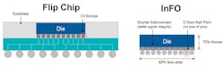
The InFO package, measuring 11.5 × 9.5 mm, uses 60% less area than a flip-chip package and is 70% thinner (Fig. 1). Xilinx also reduced the thermal and power requirements for these cost-optimized chips.
The Artix UltraScale+ supports 16-Gb/s transceivers. Also incorporated is hard logic for PCI Express (PCIe). Certification for PCIe Gen 4 support for the AU10P and AU15P is in the works. The smaller AU10P comes with 96K logic cells, 44K lookup tables (LUTs), and 3.5 Mb of RAM. Xilinx chose to keep the DSP ratio high with 400 DSP slices in the AU10P and 576 for the AU15P. Both have a dozen gigabit transceivers. Furthermore, the chips feature up to 192 Gb of aggregate bandwidth.
The Artix UltraScale+ targets applications like advanced sensor systems, high-speed networking, and ultra-compact “4K-ready” video broadcasting. The chips feature multi-level security, too, including resistance to differential-power-analysis (DPA) side-channel attacks. These security features, found across the UltraScale+ platform, also include RSA-4096 authentication, AES-CGM decryption, and Xilinx’s proprietary Security Monitor IP. The monitor adapts to security threats throughout the product lifecycle.
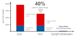
Zynq UltraScale+ ZU1 extends the low end of the SoC family. Developers can scale using higher-end SoCs like the ZU2 and ZU3. The ZU1 is available in dual and quad versions of the Arm Cortex-A53 processors. The ZU1 has been designed to use 40% less power than the ZU2, but the FPGA fabric size is only 20% less than the ZU2. It’s possible to power down unused blocks for deep sleep, consuming under 200 nW of power (Fig. 2).
About the Author

William G. Wong
Senior Content Director - Electronic Design and Microwaves & RF
I am Editor of Electronic Design focusing on embedded, software, and systems. As Senior Content Director, I also manage Microwaves & RF and I work with a great team of editors to provide engineers, programmers, developers and technical managers with interesting and useful articles and videos on a regular basis. Check out our free newsletters to see the latest content.
You can send press releases for new products for possible coverage on the website. I am also interested in receiving contributed articles for publishing on our website. Use our template and send to me along with a signed release form.
Check out my blog, AltEmbedded on Electronic Design, as well as his latest articles on this site that are listed below.
You can visit my social media via these links:
- AltEmbedded on Electronic Design
- Bill Wong on Facebook
- @AltEmbedded on Twitter
- Bill Wong on LinkedIn
I earned a Bachelor of Electrical Engineering at the Georgia Institute of Technology and a Masters in Computer Science from Rutgers University. I still do a bit of programming using everything from C and C++ to Rust and Ada/SPARK. I do a bit of PHP programming for Drupal websites. I have posted a few Drupal modules.
I still get a hand on software and electronic hardware. Some of this can be found on our Kit Close-Up video series. You can also see me on many of our TechXchange Talk videos. I am interested in a range of projects from robotics to artificial intelligence.
Comment About the Article
To join the conversation, and become an exclusive member of Electronic Design, create an account today!

Leaders relevant to this article: