Only a few years ago, the top factors when deciding which car to buy included horsepower, fuel economy, and the number of cup holders. Today, car buyers are more concerned with battery size, safety features like lane change assist, and how well their smartphone can integrate into the car’s console (OK, and the number of cup holders).
It’s no wonder that the number and variety of semiconductor devices being integrated into automobiles are exploding. Perhaps what is even more telling is how innovation in the semiconductor industry no longer is being driven primarily by computing and consumer electronics but rather by the automotive industry. Advanced networking capabilities and increasingly sophisticated safety features are driving the need for massive computing power.
Compared to other sectors, the added complication is that automotive electronics must adhere to very high quality and reliability standards as driven by the well-known ISO 26262 standard.
What’s important to realize, however, is that these quality requirements are not just necessary to maintain operational safety. In a recent consumer report on car reliability, issues related to the console’s touchscreen were among the main factors that reduced one model’s score. The quality of any of a car’s electronic components can have serious financial ramifications because it can affect both sales and maintenance costs.
Ensuring the necessary high levels of quality and reliability requires a number of solutions that span the full life cycle of automotive devices. Solutions are first needed to achieve high-quality manufacturing test. Devices then must be continuously tested in-system with failing parts extracted and analyzed to reveal the underlying defect mechanisms.
High-quality manufacturing test
By far the most common way to test logic gates in a chip manufacturing test environment is through the use of scan-based ATPG patterns. These patterns traditionally have been generated by targeting defects modeled as faults on the circuit netlist. The more basic fault models include stuck-at faults and transition faults. There have been attempts over the years to increase quality by modeling a more varied set of possible defects. Many of these new fault models unfortunately have led to a significant increase in test patterns and a corresponding increase in test time and cost.
A new fault-modeling and associated ATPG solution was introduced a few years ago that has led to significant increases in quality (reduction in DPPM) without a significant increase in test patterns. The cell-aware test approach targets specific shorts and opens internal to each library cell by locating the potential sites where a defect can occur in the physical layout and modeling it at the transistor level. Analog simulations are performed to characterize the effects of these cell-internal defects. Based on the analog simulation results, a cell-aware fault model is created that directs ATPG to generate patterns at the cell boundary targeting these internal cell defects. Silicon results across a large range of technology nodes from 350 nm to FinFETs have shown significant additional defect detection beyond standard stuck-at and transition patterns when using cell-aware ATPG.
Source: ON Semiconductor
Cell-aware test and other advanced digital test solutions are going a long way in improving device quality. It turns out, however, that the majority of field failures in automotive devices now occur within the mixed-signal portion of the chip, as illustrated in Figure 1. This is not that surprising as the successful elimination of most digital defects means that any remaining defects will likely be mixed-signal in nature. These defects, albeit often small in number, cannot be tolerated in safety-critical automotive applications. Solutions are needed to address this testing shortfall.
A basic prerequisite to automating the generation of analog tests is a means of measuring the fault coverage achieved by any test. Although fault simulation for digital circuitry has been commercially available for almost 30 years, until very recently analog fault simulation only has been discussed in academic papers and conferences. Commercial fault simulators for analog circuits are beginning to appear. The basic approach is to measure the coverage of opens and shorts and related parametric variations within a transistor-level netlist.
Coverage of a given defect is determined by evaluating a change in the circuit response in the presence of the defect through analog simulation. What makes this approach practical now is the use of a number of significant speed-up techniques to reduce the analog simulation time by several orders of magnitude over simulating each defect one at a time on the flat netlist. These techniques include such things as likelihood-weighted random sampling to ensure most time is spent simulating the most likely defects and mixed-model simulation where the highest level model or netlist is used for each subcircuit instance that does not contain the defect being simulated.
This new automation enables a number of analog test-related capabilities. First, existing analog tests can be evaluated for their effectiveness. Ineffective tests can be eliminated to reduce test time and cost. The new defect coverage metric can be used to guide the generation of new efficient tests. The approach also enables failure modes, effects, and diagnostic analysis (FMEDA)-related activities.
Analog fault simulators can be used to measure a circuit’s capability to continue to operate within acceptable operational parameters in the presence of various defects or failure modes. This analysis is very important in automotive applications because it directly relates to long-term reliability. Defect coverage metrics and FMEDA analysis are becoming hard requirements in the delivery of automotive semiconductor parts.
In-system test
Whenever a car is turned on, all the electronics are checked to ensure their proper and safe operation. This routine checking on power-up is enabled by the inclusion of a power-on self-test (POST) capability within all devices. It also is becoming necessary to periodically test safety-critical electronics during functional operation. This can be achieved by enhancing the POST infrastructure to support the capability to accept instructions from the system logic to perform various tests. This is sometimes referred to as system-initiated self-test (SIST).
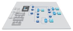
A programmable POST/SIST chip architecture is illustrated in Figure 2. An IEEE 1687 (IJTAG)-based network is used to provide access to all of the BIST controllers distributed throughout the design. This hierarchical network of scan-insertion bit switches allows for versatile and efficient communication to the controllers. An IEEE 1149.1 test access port (TAP) provides external access to the IJTAG network and primarily is used within the manufacturing test environment. A POST/SIST controller also is included in the design, which can take over the TAP signals and drive the necessary commands to any and all of the BIST controllers. Any desired sequence of tests can be executed by programming the necessary commands into a memory accessed by the controller. This memory can be dedicated or shared with other system functions. Alternatively, commands can be sent to the controller from system logic through a parallel read/write interface.
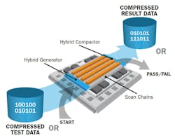
The concept of logic BIST, which involves the on-chip generation of random patterns that are applied to scan chains, has been around for many years and now is experiencing rapid adoption within automotive devices. A recent improvement to this approach has been a hybrid test solution that integrates ATPG compression and logic BIST, illustrated in Figure 3. Both solutions are typically required within automotive devices—ATPG compression for high-quality manufacturing test and logic BIST for POST and SIST.
There are clear advantages to combining the two solutions. In particular, area overhead can be reduced as the two solutions make use of similar on-chip DFT resources. For example, they both use scan chains and related test clocks. The main difference between the two solutions lies in the on-chip logic feeding test data to the scan chains and processing the test response data coming out of the scan chains. It turns out, however, that there also are similarities in this logic so the logic of the two solutions can be effectively combined to support both approaches.
An increasingly common requirement for many automotive parts is the capability to perform online memory BIST testing. The key difference between running memory BIST tests at power-on vs. online is that some form of memory access arbitration is required between the functional logic and the BIST controller.
A handshaking protocol can be implemented within the memory interface logic to handle this. The handshaking protocol and BIST controller together can implement either destructive or nondestructive testing. Destructive testing generally is used during manufacturing test. In this case, the handshaking logic disables the memory from functional use so the memory BIST controller can carry out its full test uninterrupted. Although this is the simplest approach, destructive testing has the significant drawback of affecting system performance because the memory under test is not available for a significant period of time.
There also is the added overhead of saving the memory pretest content to another location and restoring the memory once the testing is complete. In contrast, during online testing, the memory BIST controller tests the memory using a series of short sequences of transactions, often referred to as bursts. A burst typically will only last for a small number of clock cycles (perhaps 20 to 30) and targets different memory locations each time. The entire memory is therefore tested over a large number of short memory BIST sessions. The approach is nondestructive because the memory locations that are modified by a burst are saved and restored during each burst by the MBIST controller. Functional performance is not significantly affected because the bursts are only initiated when the arbitration logic determines the memory is free.
Field return analysis
The automotive market is very sensitive to the occurrence of any in-field failures. These failures need to be quickly understood, and the possibility of similar failures occurring eliminated. This, in turn, requires a methodology for the fast and accurate identification of the root-cause defect behind each failure.
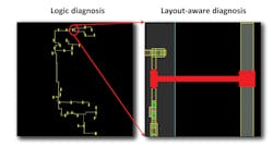
Scan test diagnosis is one such methodology for finding the location of a logic defect in a failing die. Using ATPG test patterns and the design description, diagnosis turns failing test cycles into valuable data. However, even with significant improvements in scan logic diagnosis algorithms over the years, there is a gap between what scan logic diagnosis can deliver and what failure analysis engineers need to quickly identify defects. This deficiency is addressed by the more recent layout-aware diagnosis approach that leverages the physical design information, generally in the form of Library Exchange Format and Design Exchange Format files, to significantly improve the accuracy and resolution of the diagnosis results, as illustrated in Figure 4.
Using the layout data enables meaningful defect classification and enhanced diagnosis reporting that include net segments and defect bounding boxes. This also enables correlation of diagnosis results with other design profiling information like design rule and lithographic violations.
Conclusion
Because of the nature of the input data used, the diagnostic solutions can only identify interconnect defects and defective cells. In practice, many defects affect only the internal logic of cells, such as polysilicon contacts. A new approach called cell-aware diagnosis extends diagnosis to include internal cell defects. This is enabled by characterizing a cell library similar to what is needed for cell-aware ATPG but with more information for diagnosis such as layout data. Diagnosis results include layout marker files for cell internal suspects which can be viewed in a GDS viewer and used to obtain X/Y coordinates to guide physical failure analysis. Apart from physical localization, internal cell diagnosis also exposes some defects that otherwise would never be identified.
Meeting automotive quality and reliability requirements such as those driven by the ISO 26262 standard will only become more difficult as device sizes and complexities continue to grow. Advanced test technologies provide key building blocks toward ensuring compliance with the new standards. Adoption of these capabilities not only will improve the capability of semiconductor manufacturers to achieve necessary quality and reliability metrics, but also will help to further differentiate their products by delivering embedded test capabilities that can be leveraged by their customers at the system level and in the field.
About the author
Stephen Pateras is product marketing director within the Mentor Graphics Silicon Test Solutions group and has responsibility for the company’s ATPG and DFT products. He received his Ph.D. in Electrical Engineering from McGill University in Montreal, Canada. [email protected]


