The Hot Chips Symposium is where the cutting-edge technology appears, and this year is no different. Parallel processing is the name of the game, especially when it comes to 5G and machine-learning (ML) solutions.
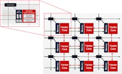
We got a more detailed glimpse at Xilinx’s “Everest” adaptive compute acceleration platform (ACAP) that targets 5G and ML. ACAP is a tile-based architecture that’s commonly found in high-performance computing and network processing (Fig. 1). The non-blocking interconnect delivers over 200 GB/s/tile and adjacent cores can also share results. The instruction set includes integrated synchronization primitives. Like an FPGA, the system is scalable, allowing large arrays to tackle more ambitious projects.
1. Xilinx’s adaptive compute acceleration platform (ACAP) is built around a tile-based network of parallel processors.
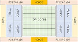
Tachyum’s Prodigy chip targets networking applications with a pair of 400-Gb Ethernet links to feed its 64-core chip (Fig. 2). It’s designed to address ML applications that are becoming increasing important in managing and delving into the contents of network traffic. The cores use out-of-order (OOO) execution courtesy of the compiler. It implements instruction parallelism by applying poison bits. All of the I/O is linked via a high-speed ring that also connects to the multicore fabric.
2. Tachyum’s Prodigy chip sports a 64-core array with 400-Gb Ethernet support to handle networking tasks.
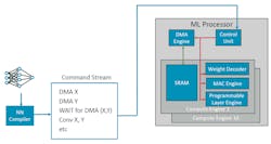
On another front, Arm lifted the veil more on its ML processor. It includes features like static scheduling, where convolution operations wait until data is DMA’d into memory, providing relatively predictable performance (Fig. 3). Convolution output feature maps are interleaved across compute engines; weight and feature map compression support reduce data and power requirements.
3. Arm’s machine-learning processor can synchronize convolution operations with DMA transfers.
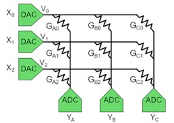
Mythic explained its matrix multiplying flash-memory technology designed to deliver deep-neural-network support on the edge using a fraction of the power needed by alternatives. The hybrid digital/analog array performs calculations with in the memory array where the network weights are stored. ADCs are used to read a memory cell’s voltage-variable conductance resulting in an 8-bit value rather than the one or two bits normally stored in a cell (Fig. 4). The architecture is designed to support ML models like those developed using TensorFlow.
4. Mythic drives its memory matrix with DACs and reads results using 8-bit ADCs.
The integration of ML in almost every application space is placing demands on hardware and software. These and other technologies are rising to meet the demand.
About the Author
William G. Wong
Senior Content Director - Electronic Design and Microwaves & RF
I am Editor of Electronic Design focusing on embedded, software, and systems. As Senior Content Director, I also manage Microwaves & RF and I work with a great team of editors to provide engineers, programmers, developers and technical managers with interesting and useful articles and videos on a regular basis. Check out our free newsletters to see the latest content.
You can send press releases for new products for possible coverage on the website. I am also interested in receiving contributed articles for publishing on our website. Use our template and send to me along with a signed release form.
Check out my blog, AltEmbedded on Electronic Design, as well as his latest articles on this site that are listed below.
You can visit my social media via these links:
- AltEmbedded on Electronic Design
- Bill Wong on Facebook
- @AltEmbedded on Twitter
- Bill Wong on LinkedIn
I earned a Bachelor of Electrical Engineering at the Georgia Institute of Technology and a Masters in Computer Science from Rutgers University. I still do a bit of programming using everything from C and C++ to Rust and Ada/SPARK. I do a bit of PHP programming for Drupal websites. I have posted a few Drupal modules.
I still get a hand on software and electronic hardware. Some of this can be found on our Kit Close-Up video series. You can also see me on many of our TechXchange Talk videos. I am interested in a range of projects from robotics to artificial intelligence.


