What’s Inside a Wireless IoT SoC?

The IoT continues to expand, but engineers continue to wrestle with a web of challenges: fragmented standards, tight constraints on power and space, and constant tradeoffs between performance and cost. However, a new wave of wireless SoCs is untangling these issues. By bringing together wireless connectivity, computing, and security, these IoT chips can help reduce hardware complexity and time-to-market for everything from sensors embedded on factory floors to smart-home devices, said Silicon Labs CTO Daniel Cooley.
“You’re eventually not going to have a wireless application that doesn’t have some degree of processing in it,” he said in a briefing with reporters at Silicon Labs’ 2025 Works With conference in Austin, Texas, last month.
Last month, Silicon Labs introduced the first chips in its Series 3 platform — its vision for the future of IoT SoCs. The new chips will support a wide range of long- and short-range wireless protocols, including Wi-Fi, Bluetooth, and Thread. Many of them are specifically designed to work with the Matter standard to bridge the gap between them.
By upgrading from 40 nm to 22 nm, the company said Series 3 brings generational gains in computing, connectivity, and security to the table, outperforming the capabilities of its Series 2 platform without replacing it.
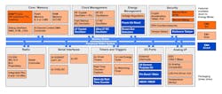
No single chip is ideally suited for every IoT device — the design requirements are too diverse. But Cooley explained that the Series 3 platform features the fundamental building blocks for connecting these devices to the IoT. These comprise:
- Wireless connectivity, including the RF transceiver as well as power amplifiers (PAs), RF switches, LNAs, and most or all other RF front-end components plus interfaces to external PAs.
- Application processor, typically a Cortex-M MCU that’s increasingly used to run real-time operating systems (RTOS) and comes paired with more on-chip memory to manage the complexity.
- AI accelerators, through a neural processing unit (NPU) or hardware accelerator to run AI and machine-learning (ML) models more efficiently than software running on the MCU.
- Hardware security, based on a secure enclave that acts as a hardware root of trust (RoT) and runs cryptographic operations to help keep hackers out of the system.
- Sensor interfaces, including serial interfaces and general-purpose I/Os, supplemented by analog-to-digital converters (ADCs) and other parts of the analog front end (AFE) to capture the data.
- Peripherals, for saving PCB space and reducing the cost of integrating external components. For instance, it integrated LED pre‑drivers in its SiMG301 to control dimming in smart lighting.
By focusing in on the demands of IoT devices, Cooley said it distilled everything in the Series 3 — starting with its SiXG301 and SiXG302 — into a platform purpose-built for secure, robust, intelligent connectivity without excessive power and cost.
“We are focused on IoT connectivity, and we are squarely focused on this one market,” noted Cooley. “We have the widest portfolio of wireless technologies, and we believe that we're the technology leader in the space.”
Silicon Labs is betting that its IoT focus gives it the engineering edge over other companies that spread out its R&D over several different markets. “We don't have those distractions — in terms of the level of investment in the company—and so we don’t have to dilute what we're doing when it comes to our chip-level engineering,” said Cooley. “We make technology decisions because we know exactly what we're going into. There is nothing we're doing that our competitors can't do, but long-term, we think we’re ahead.”
The Move to Multiprotocol Wireless SoCs
The IoT is running into a wall of wireless complexity that the latest SoCs are equipped to solve, according to Cooley.
Today, IoT devices use a wide range of wireless protocols that operate in overlapping or very close frequency bands, which can potentially cause RF interference, signal degradation, and increased latency. Each protocol plays a distinct role: For instance, in a connected door lock, users can pair it with a smartphone over Bluetooth; control it remotely and connect it to the cloud using Wi-Fi; and integrate it to home automation through Thread for mesh networking. Many IoT devices must rapidly shift between protocols or run them at the same time.
“It’s a multiprotocol world,” said Cooley. “There will never be one wireless protocol to rule them all.”
To cut through the tangle of wireless technologies, companies are racing to roll out chips that can handle several different protocols at a time — integrating Wi-Fi and Bluetooth, Bluetooth and Thread, and Wi-Fi, Bluetooth, Thread, and Zigbee, among others. These chips are all about reducing hardware complexity and saving PCB space, which is critical for compact IoT devices, while managing complex protocol stacks and reducing the RF interference between them all.
The first multiprotocol Series 3 SoC — the SiMG301 — brings Bluetooth LE, Zigbee, and Thread into a single chip that’s targeted at smart lighting and other line-powered smart plugs, sensors, switches, and controllers.
At the heart of it is the high-performance 2.4-GHz radio that offers up to +10 dBm of transmit (TX) power while supporting −98.6 dBm of receive (RX) sensitivity for Bluetooth and −106.3 dBm for Thread and other protocols that use the 2.4-GHz band. This reduces the impact of interference in increasingly crowded RF areas like smart homes.
“If you could hear what is happening in the 2.4-GHz band, it would sound like this cacophony of clicks and chirps,” said Cooley. “We have very high-performance, congestion-tolerant radios.”
It uses a separate radio CPU core to control all of the wireless connectivity, from the protocol stacks to the firmware that enables it to shift between protocols dynamically or run protocols such as Zigbee and Thread at the same time using its “concurrent multiprotocol” technology. That enables continuous communication between IoT devices, regardless of the protocols in use, and allows for backwards compatibility. By bringing Bluetooth and Matter over Thread into a single chip, it saves space for additional integrations like Wi-Fi.
The SIMG301 has a scalable PA architecture. In high-power mode, the PA provides a +10-dBm output for maximum range or signal strength; in low-power mode, the PA output is 0 dBm for optimized power.
Transforming the RF SoC into the IoT SoC
The first generation of IoT radios required external co-processors to run applications. But now most wireless SoCs come with a dedicated processor, which makes it easier for engineers to develop Matter-ready IoT devices.
Like many major IoT chip companies, Silicon Labs is betting on Matter to become the standard way for the smart home to communicate. It would unite a market that has long been fragmented by the lack of compatibility between devices from different manufacturers and linked by different wireless protocols. Such compatibility problems pushed Apple, Google, Samsung, and a wide swathe of semiconductor firms (including Silicon Labs) to create the open standard through the Connectivity Standards Alliance (CSA).
The standard, which started as part of Project Connected Home over IP (Project CHIP), enables everything from smart thermostats to smart door locks, switches, and lighting to connect locally without using the cloud.
The SiMG301 is one of the first chips in the CSA’s Matter Compliant Platform Certification program, as it comes with a software development kit (SDK) that’s been certified with the hardware for core Matter functionality. By building on top of a certified platform, Silicon Labs said engineers can inherit pre‑tested commissioning, networking, and security, cutting down on the complexity, cost, and time required for product certification.
Series 3 is based on a multicore architecture that separates application processing from wireless connectivity and security, giving it headroom to handle larger wireless protocol stacks and more computationally intense jobs. The SiMG301 features a Cortex-M33 clocked at up to 150 MHz that’s supplemented by a relatively large amount of memory: up to 4 MB of co-packaged flash for program memory and 512 kB of on-chip RAM for data memory.
It's also integrating more general-purpose I/Os to interface with the sensors embedded in many edge devices as well as other AFE components to convert and condition analog signals from the sensors.
Silicon Labs plans to integrate its second-generation Matrix Vector Processor in several of its Series 3 SoCs to enable fast, power-efficient execution of AI. That parallels what it did with its most advanced Series 2 SoC, the MG26. It uses hardware accelerators to offload machine-learning operations off of the main CPU, specifically ones for audio, vision, and other sensor-powered features, such as keyword spotting and motion detection. The NPU is up to 10X faster while using 80% less power than the CPU alone, drastically reducing power draw in wireless IoT devices.
Series 3 integrates a power management unit (PMU) on-chip to boost efficiency, which is bound to be even more important in Silicon Labs’ SiXG302 family for battery-powered IoT devices, due out in 2026.
Hardware-Secure Connectivity for the IoT
As more unconnected “things” are connected to the IoT, security at the hardware level is becoming critical, said Cooley.
The SiXG301 family features the company’s latest secure vault for IoT security. The secure enclave comes with what Silicon Labs calls the first PSA Level 4 certification, the highest level recognized by PSA Certified.
Silicon Labs said the secure vault “raises the bar for edge protection” by defending against physical attacks such as laser fault injection, side-channel analysis, micro-probing, and voltage manipulation. It incorporates a hardened RoT, lifecycle controls, and secure OTA updates for devices that can be deployed for a decade at a time. The Series 3 SoCs also feature a quad-SPI (QSPI) memory interface with run-time authentication and encryption.
The secure vault in the Series 3 SoCs help developers reach compliance with emerging regulations, including the EU's RED and CRA and the U.S. Cyber Trust Mark, among others.
“Our parts are ready for all of this,” Cooley remarked about the tightening IoT security regulations. “We don't have to reengineer the entire portfolio because it requires circuitry down into the hardware. You need a physically unclonable function (PUF), you need a hardware root of trust, and you need cryptographic key management. These are not just software solutions.”
One of its latest innovations relates to execute-in-place (XIP), in which the processor executes code directly from external flash instead of copying it to on-chip memory first. The Series 3 secure vault authenticates the code as it enters the processor.
“In a world where IoT devices are more feature-rich and adopting real-time operating systems, you have to enable memory expansion, and so now we have basically the world's most secure serial memory interface, and we can prove it,” said Cooley.
The Future of IoT SoCs is All About Integration
With the demand for wireless connectivity on the rise, companies are adding more of everything to these SoCs, from radios and memory to processors, to enable more intelligent connectivity while balancing power and cost. While others are adopting FD-SOI, Silicon Labs said it’s upgrading to more advanced CMOS nodes such as 22 nm to not only reduce area, but also to save space to integrate more features and more memory in the same package.
Cooley said there will be a higher degree of integration in the future. “We’re able to take advantage of the benefits of Moore’s Law. But this is the last Bulk CMOS node and then it’s down to FinFET.”
About the Author

James Morra
Senior Editor
James Morra is the senior editor for Electronic Design, covering the semiconductor industry and new technology trends, with a focus on power electronics and power management. He also reports on the business behind electrical engineering, including the electronics supply chain. He joined Electronic Design in 2015 and is based in Chicago, Illinois.
Comment About the Article
To join the conversation, and become an exclusive member of Electronic Design, create an account today!

Leaders relevant to this article: