The Elusive Blue LED: How Did Researchers Finally Triumph?
What you'll learn:
- How the blue LED was created.
- The history of attempts and challenges in making it happen.
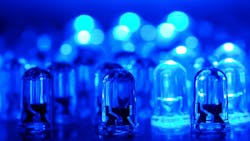
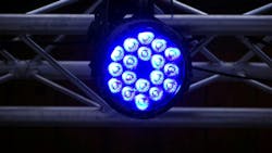
It’s hard to believe that the first blue LED didn’t arrive until 1993. They look simple, but looks are deceiving (Fig. 1).
James R. Biard and Gary E. Pittman, Texas Instruments engineers, accidentally created the first LED in 1961. At the time, they collaborated on a project, developing low-noise parametric amplifiers for X-band radar receivers, and found a diode they created on a gallium-arsenide substrate that emitted infrared light. In 1962, the SNX-100 GaAs LED, the first commercial LED, was released. That same year, GE physicist Nick Holonyak created the first red LED.
Producing various LED colors involved applying electric currents to materials with distinct molecular structures. Researchers observed how the energy bandgap of each material influenced wavelength, and therefore, the color of the emitted light.
Experimenting with different compounds was a lengthy trial-and-error process. Using the right compound meant it had to efficiently generate photons and remain thermally stable to prevent degradation under electric currents. In addition, the compound needs to be manufactured efficiently and at scale.
The Elusive Materials for a Blue LED
Creating red and green LEDs with the right materials was achieved in the early production stage. However, finding a material for the blue LED was more difficult as it required the widest bandgap. Typically, LEDs were developed using materials like gallium arsenide phosphide (GaAsP) and gallium phosphide (GaP), which generated red, orange, yellow, and green light. Finding the right compound to generate light with a blue wavelength remained elusive.
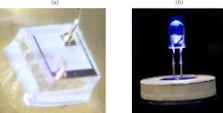
In the early 1970s, zinc selenide (ZnSe), a II-VI semiconductor that has an approximate bandgap of 2.7 eV, ideal for blue emission (460 nm), was researched for LED applications (Fig. 2). LEDs using ZnSe technology had limited efficiency due to material quality challenges, often lasting only hours or days before failing.
ZnSe technology’s short lifespan was due to the material not being thermally or chemically stable, leading to rapid defects and degradation. It also had limited internal quantum efficiency as the dislocation density often surpassed 108 cm-2. This made it impossible to brightly illuminate ZnSe devices for a long time for commercial applications.
Research into a GaN-Based Solution
Due to those imperfections, Herb Maruska and Wally Rhines, Stanford University engineers, turned to gallium nitride (GaN), a III-V semiconductor with a direct bandgap of roughly 3.37 to 3.4 eV. They believed GaN served as a perfect solution for blue emission.
However, it was very challenging to use as GaN can’t grow as a bulk single crystal because it decomposes at high temperatures before melting and it doesn’t have a lattice-matched substrate. Growing GaN on sapphire results in the lattice mismatch reaching between 13% to 16%. This caused it to have high threading dislocations on the order of 1010 cm-2. Defects like these effectively destroyed light emissions due to non-radiative recombination.
>>Download the PDF of this article

GaN crystals grow via metal-organic chemical vapor deposition (MOCVD) at temperatures ranging between 1,832 and 1,922°F for the main epitaxial growth layers. Optimizing crystalline quality and layer uniformity is achieved by carefully controlling temperature gradients, gas flow rates, and precursor materials such as trimethylgallium (TMG) and ammonia (NH3).
To eliminate lattice strain, scientists introduced low-temperature buffer layers of aluminum nitride (AIN) or GaN approximately 20 to 50 nm thick, deposited at lower temperatures (−868 to 1,472°F). With this approach, dislocation densities shrank from 1010 cm-2 to the mid-108 cm-2.
Growing high-quality GaN proved inefficient as p-type doping was difficult to achieve. Although scientists have used silicon donors for n-type doping, it was challenging to produce free holes for p-type conductivity. Magnesium served as the dopant, but the Mg acceptors were passivated by hydrogen atoms added during MOCVD growth, suppressing the p-type activity. Attempting to produce p-type GaN formed a resistive, non-conductive material.
Optimizing GaN Growth with Customized MOCVD
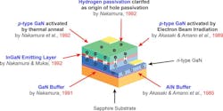
Building on those discoveries, Shuji Nakamura developed a new custom-designed MOCVD technology to optimize all of the GaN growth steps. In 1991, he designed the two-flow MOCVD reactor, which introduced a secondary downward inert gas flow perpendicular to the reactive gas flow onto the substrate surface. The secondary flow suppressed thermal convection within the reactor, decreasing turbulence that formed powdery deposits and uneven GaN growth.
Enhancing these gas flow dynamics also improved the thermal boundary layer close to the substrate, leading to reproducible, even, and high-quality GaN crystal growth on 2-in. sapphire substrates (Fig. 3).
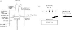
During experiments, Nakamura grew GaN crystals in temperatures reaching approximately 1,832°F with reactor pressures near 200 Torr. Under those conditions, the V/III precursor ratios surpassed 5,000, which helped stabilize the nitrogen-rich atmosphere essential to produce smooth GaN layers. N-type doping silicon concentrations remained at 1018 cm-3.
The magnesium-doped (similar levels) p-type layers underwent post-growth annealing at 752 to 932°F in nitrogen or low-energy electron beam irradiation (LEEBI), dissociating Mg-H complexes to activate the Mg acceptors. Activating those holes led to the production of efficient GaN p-n junctions, allowing light to illuminate in bright blue.
Nakamura then made a breakthrough by adding indium into the active layer, which formed indium gallium nitride (InGaN). Implementing InGaN layers with varying indium content (approximately 10% to 20%) enabled emission wavelength tuning from violet (around 400 nm) to blue (around 470 nm) (Fig. 4).
However, because indium has a larger atomic radius (approximately 20%) than gallium, the alloying produces more strain. This meant growth parameters needed precise control to eliminate the risk of defects. The team grew the InGaN layers as multiple quantum wells (MQWs) via MOCVD at 1,472 to 1,652°F, changing 2- to 3-nm-thick InGaN wells to 1- nm barriers, isolating electrons and holes within narrow areas to boost radiative recombination efficiency. As a result, non-radiative losses from defects shrank.
Another problem occurred with the MQW’s internal electric fields. The wurtzite GaN crystal’s piezoelectric and spontaneous polarization caused strong band bending across the wells, an effect called the quantum-confined Stark effect (QCSE). QCSE splits electron and hole wavefunctions, making the recombination less efficient.
To address this issue, engineers shrank the well thickness and precisely fine-tuned the indium composition, balancing strain and confinement. This ensured minimal QCSE and maintained high emission intensity.
Entering the Wafer Processing Stage to Produce LED Chips
After completing the epitaxial growth of InGaN and GaN layers via MOCVD, the wafers underwent key processing steps to produce LED chips. Photolithography sets the LED mesas and device patterns before reactive ion etching (RIE) with chlorine gases for layer etching and isolating devices.
Metallization produces ohmic contacts essential for electrical injection. That involves depositing and patterning titanium/aluminum (Ti/Al) layers on n-type GaN. Meanwhile, p-type GaN has nickel/gold (Ni/Au) layers. The team then enhanced the contact properties through post-deposition annealing at 752 to 932°F.
Deploying surface-roughening techniques and patterned sapphire substrates (PSS) enhances light extraction efficiency. PSS decreased dislocation densities during growth and produces micro- or nanoscale textures to minimize total internal reflection. This increased the output of generated light. Such wafer improvements are crucial to ensure blue LEDs have high brightness and efficiency.
The First High-Brightness Blue LED
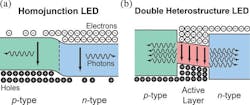
It wasn't until 1993 that Nakamura and his team finally developed the first-ever high-brightness blue LED. Their invention had a double heterostructure, placing an InGaN active layer between n-type and p-type GaN layers (Fig. 5). They used an Si-doped InGaN with a thickness of around 20 nm. It also had an emission wavelength of approximately 440 nm, generating bright blue light. This blue LED had an optical power of 125 µW with an external quantum efficiency (EQE) of 0.22% at a forward current of 20 mA.
Even today, manufacturing GaN LEDs involves the right balance of chemistry and precision. MOCVD grows the epitaxial layers while gallium and indium are distributed through trimethylgallium and trimethylindium, with ammonia serving as the nitrogen source.
Growth occurs at approximately 1 to 5 µm/hour, and the whole process takes a few hours to complete an epitaxial stack. Precisely adjusting doping concentrations enables control of carrier densities and junction behavior.
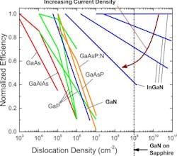
The past 20 years also saw improvements that increased EQE from a small percentage to over 80% in commercial devices, thanks to enhancements in internal quantum efficiency through strain engineering, quantum wells optimization, and nanostructural light patterns. The carrier localization in the InGaN alloy enabled more tolerable dislocation densities.
Steps to Overcome Lingering Challenges with GaN LEDs
GaN LEDs still faced challenges due to crystallographic defects like threading dislocations (107 to 1010 cm-2), stacking faults, and V-defects. These served as non-radiative recombination hubs that shrank internal quantum efficiency. Sometimes, V-defects isolated carriers and mitigated efficiency loss.
Meanwhile, internal InGaN quantum wells had point defects and impurities that degraded efficiency by producing deep traps, enabling non-radiative recombination. Refining the use of InGaN or InAlN underlayers beneath the quantum wells improved performance by reducing point-defect formation.
Shockley-Read-Hall, Auger, and density-activated defect recombination contribute to efficiency droop, making them crucial for high injection currents. Those effects have been minimized due to advances in reduced defect densities, enhanced epitaxy, and quantum-well design. LED devices last longer as they have improved thermal management, passivation through atomic layer deposition, and neutral-beam or chemical etching to reduce sidewall damage (Fig. 6).
Shuji Nakamura’s contribution to blue LEDs revolutionized lighting by enabling efficient white lights and blue laser diodes in Blu-ray technology. This effort overcame decades of materials challenges involving GaN and embodied a milestone in engineering that paved the way toward solid-state lighting and display technologies.
So, after all of this, what do we do when we see a blue LED on a device? We put a piece of tape over it.
>>Download the PDF of this article
About the Author

Cabe Atwell
Technology Editor, Electronic Design
Cabe is a Technology Editor for Electronic Design.
Engineer, Machinist, Cartoonist, Maker, Writer. A graduate Electrical Engineer actively plying his expertise in the industry and at his company, Gunhead. When not designing/building, he creates a steady torrent of projects and content in the media world. Many of his projects and articles are online at element14 & SolidSmack, industry-focused work at EETimes & EDN, and offbeat articles at Make Magazine. Currently, you can find him hosting webinars and contributing to Electronic Design and Machine Design.
Cabe is an electrical engineer, design consultant and author with 25 years’ experience. His most recent book is “Essential 555 IC: Design, Configure, and Create Clever Circuits”
Cabe writes the Engineering Life & Engineering on Friday blog on Electronic Design.
See Cabe's cartoons & comic strips here.
Comment About the Article
To join the conversation, and become an exclusive member of Electronic Design, create an account today!

Leaders relevant to this article: