What you'll learn:
- Discover the new USB standards known as eUSB2 and eUSB2V2.
- What are the differences between USB 2.0, eUSB2, and eUSB2V2?
- Understand the advantages of eUSB2 and eUSB2V2 for modern embedded and edge AI designs.

If eUSB2 — or its newer variant, eUSB2V2 — is new to you, you’re not alone. These USB-based interfaces are still emerging, but they matter now more than ever to engineers building 5-nm and more advanced SoCs, or connecting one of these chips to a more mature-node companion. They’re particularly relevant in edge AI and other embedded systems, where massive amounts of data pinball between components.
At a high level, eUSB2 is USB 2.0 reworked for the demands of modern silicon. eUSB2 was introduced through the efforts of the USB-IF to modernize the USB 2.0 standard, starting in the mid-2010s.
Referred to as eUSB2 (or eUSB2 version 1), the first version preserved USB 2.0 signaling and software compatibility but replaced the traditional PHY with a lower voltage, SoC‑friendly implementation.
As the demand for greater data rates in edge AI applications grew, along came eUSB2 Version 2 (eUSB2V2) in late 2024, boosting performance up to 4.8 Gb/s while retaining USB 2.0 ecosystem backward compatibility. For many designs, eUSB2V2 is the simplest way to hit power and performance targets without jumping all the way to USB 3.x.
What Exactly is eUSB2?
Think of eUSB2 and eUSB2V2 as USB 2.0 redesigned for inside-the-box connections. eUSB2 drops the traditional 3.3-V I/O requirement down to ≤1.2 V, which is critical for advanced‑node SoCs. It’s optimized for embedded chip‑to‑chip links rather than external links. It also supports tighter power, electromagnetic interference (EMI), and RF interference (RFI) noise budgets.
eUSB2V2 builds on that foundation. In addition to the 480-Mb/s mode, it supports up to 4.8 Gb/s in one direction while keeping the reverse direction slower and more efficient. Depending on your system, eUSB2 can be used natively between chips or through a repeater to connect to legacy USB 2.0 devices.
>>Download the PDF of this article, and check out the TechXchange for similar articles and videos


Typical use cases include AI PCs, edge AI-enabled IoT devices, and wireless products pairing advanced and mature process nodes.
How Fast are These Interfaces, and What Link Modes are Available?
- eUSB2 (v1): Up to 480 Mb/s similar to legacy USB 2.0.
- eUSB2V2: Introduces HSx modes ranging from approximately 960 Mb/s up to 4.8 Gb/s.
One of the most practical advantages of eUSB2V2 is flexibility. You can run links symmetrically (the same speed in both directions) or asymmetrically. For example, a camera streaming video upstream might run at multi‑Gb/s, while the return path stays at 480 Mb/s. This flexibility allows you to match the link to real traffic patterns rather than overengineering the interface.
What’s Wrong with USB 3.x? Why Not Use It Instead?
USB 3.x is an excellent choice for external ports and very high-throughput applications. But it also comes with significantly higher PHY complexity, power consumption, and EMI/RFI noise challenges.
For many internal connections (debug links, cameras, and localized data paths), USB 3.x can be more than what is actually necessary. eUSB2 and eUSB2V2 are positioned between USB 2.0 and USB 3.x, offering multi‑Gb/s performance with a simpler, lower‑power implementation that’s better suited for embedded environments.
What are the Differences Between USB 2.0, eUSB2, and eUSB2V2?
The key differences separating these USB variants are highlighted in Figure 1. USB 2.0 supports data rates up to 480 Mb/s and uses a 3.3-V I/O voltage in the PHY.
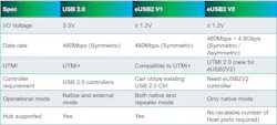
eUSB2 keeps the USB 2.0 protocol and the same 480-Mb/s data rate but shifts to a low I/O voltage (around 1.2 V or less) optimized for advanced-node SoCs. It supports both chip-to-chip connections and external USB 2.0 ports through repeater mode. eUSB2V2 further extends this concept by boosting data rates up to 4.8 Gb/s, targeting higher‑bandwidth, chip‑to‑chip interconnects only.
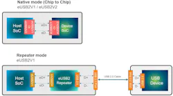
Is eUSB2 Only Targeted at Embedded Connections?
Not entirely. While eUSB2V2 is intended strictly for internal, chip‑to‑chip links, eUSB2 v1 can support both internal connections and external USB 2.0 ports (Fig. 2).
Where Will eUSB2V2 Add the Most Value?
eUSB2V2 is a strong fit for new edge AI designs that need higher bandwidth but can’t afford higher power or added noise. In AI PCs and edge systems, large amounts of data move continuously among sensors, high‑resolution cameras, AI accelerators, and advanced-node SoCs. eUSB2V2 supports these faster chip‑to‑chip links efficiently, helping designers meet performance goals without the power, noise, and complexity tradeoffs of USB 3.x.
eUSB2V2 is particularly well-suited for high-resolution cameras in AI PCs and edge systems, as well as connecting advanced-node SoCs to mature-node companions.
How Does eUSB2V2 Help with Power and EMI/RFI Noise Issues?
Power efficiency and EMI/RFI noise reduction are key design goals for eUSB2V2, especially for modern edge AI systems. One of the primary means to achieve this is asymmetric link operation, where each direction runs only as fast as needed.
In many real-world designs, such as connecting a camera to a processor, most of the data moves in one direction. eUSB2V2 enables a high-traffic path to operate at up to 4.8 Gb/s, while keeping the return path at a much lower speed for control and status data. This reduces high-speed switching activity, thereby lowering overall power. It also limits high-frequency noise sources on the board, helping manage EMI and RFI.
Do eUSB2 and eUSB2V2 Still Use UTMI?
Yes, mostly.
eUSB2 v1 continues to use the familiar UTMI/UTMI+ interface. eUSB2V2 introduces UTMI 2.0, designed to support higher data rates and flexible link configurations beyond the 480-Mb/s limit.
Is There Working Silicon for These New Standards?
Yes. Several public demos of complete end‑to‑end eUSB2V2 systems have taken place, including FPGA‑based host and device controllers and a PHY implemented in a 3-nm test chip. This demo, shown at CES 2026, runs real workloads such as live 4K video in raw format, streaming (UVC) alongside recorded video (bulk data) transfers — demonstrating both performance and interoperability at the system level.
When Should I Consider Using eUSB2 v1 Over eUSB2V2?
The decision mainly comes down to two factors: how much bandwidth you need, and what the USB port is connecting to, namely, internal chip‑to‑chip links or external devices.
You may want to stick with eUSB2 v1 if:
- Your bandwidth needs are comfortably below 480 Mb/s. In this range, eUSB2 is simpler and more than sufficient.
- You must connect directly to external hubs or legacy USB devices, which requires standard USB compatibility.
What are Some Recommendations for System Designers?
If your design depends on USB 2.0 but targets an advanced-node SoC or needs to connect to one, and USB 3.x feels heavier than necessary, eUSB2 (especially eUSB2V2) is worth a serious look. It delivers multi‑Gb/s internal bandwidth using low‑voltage, embedded‑friendly signaling, without the cost and complexity of a full SuperSpeed stack.
Rather than replacing external USB 2.0, eUSB2 complements it by offering a more balanced option for modern embedded and edge AI designs.
>>Download the PDF of this article, and check out the TechXchange for similar articles and videos
About the Author

David Shin
Senior Product Marketing Manager, Consumer Interface IP, Cadence,
David Shin is a senior product marketing manager at Cadence, where he specializes in interface IP for the consumer segment, including ubiquitous USB IP.
Before joining Cadence, David worked as a product line management professional at Cypress Semiconductor (now part of Infineon), Synaptics, and Omnivision. In these roles, he defined and developed cutting-edge device solutions such as USB products, touchscreen controllers, fingerprint sensors, and CMOS image sensors for applications including smartphones, IoT, and AR/VR/MR in the metaverse.
David holds a master’s degree in computer science from California State University, Chico.
Comment About the Article
To join the conversation, and become an exclusive member of Electronic Design, create an account today!

Leaders relevant to this article: