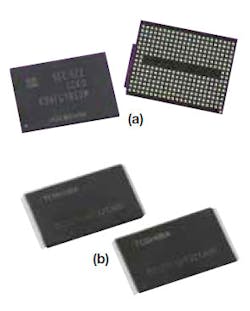
Storage vendors were showing off their latest wares at the Flash Memory Summit. This includes devices like Samsung’s 3D, 48-layer V-NAND chip [Fig. 1(a)] that packs in 256 Gbits of 3-bit multi-level-cell (MLC) flash memory. That is 32 Gbytes on a single chip. Not to be outdone, Toshiba’s BiCS 48-layer, 3-bit MLC flash chip [Fig. 1(b)] also has 256 Gbits of storage. Samsung’s cell uses a 3D Charge Trap Flash (CTF) structure.
Also be sure to check out our gallery coverage of the event, here.
Toshiba also announced a 16-layer NAND flash device that uses Through Silicon Via (TSV) technology. This allows the chip to transfer data at rates in excess of 1 Gibt/s. The approach also cuts power requirements in half by reducing core voltage to 1.8 V and I/O to 1.2 V. While the 48-layer devices will provide high capacity, the TSV chips deliver low latency and high bandwidth and the chips have a high IOPS/W.
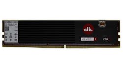
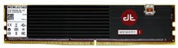
Riccardo Badalone’s, chief executive officer and co-founder of Diablo Technologies, kicked off the conference with his keynote, “Disruptive Memory Technology Enables New In-Memory Applications.” Of course, he was talking about Diablo Technologies’ new DDR4 Memory1 DIMM (Fig. 2). Memory1 DIMMs are available with capacities up to 256 Gbytes. That is four times the storage available in DRAM DIMMs and the flash memory is on the memory channel, not the PCI Express bus (see "Memory Channel Flash Storage Provides Fast RAM Mirroring").
Seagate was touting its PCIe Gen 3, NVMe support with its Nytro XF1440 2.5-in and Nytro XM1440 M.2 SSDs that deliver 25,000 IOPS/W. The hot swappable drives use a SFF-8639 connector and have a maximum capacity of 1.8 Tbytes while the M.2 devices support up to 960 Gybtes. Self-Encrypting Drives (SEDs) are available.
There was discussion of Intel and Micron’s XPoint 3D storage and Altera was demonstrating its NAND Flash reference design that can extend the life of flash memory up to 7 times. The reference design used an Arria 10 SoC and implemented Mobiveil's Universal NVM Express Controller (UNEX).
There was never a dull moment at Flash Memory in Santa Clara.
About the Author
William Wong Blog
Senior Content Director
Bill's latest articles are listed on this author page, William G. Wong.
The latest blogs have been moved to alt.embedded on Electronic Design.
Bill Wong covers Digital, Embedded, Systems and Software topics at Electronic Design. He writes a number of columns, including Lab Bench and alt.embedded, plus Bill's Workbench hands-on column. Bill is a Georgia Tech alumni with a B.S in Electrical Engineering and a master's degree in computer science for Rutgers, The State University of New Jersey.
He has written a dozen books and was the first Director of PC Labs at PC Magazine. He has worked in the computer and publication industry for almost 40 years and has been with Electronic Design since 2000. He helps run the Mercer Science and Engineering Fair in Mercer County, NJ.
- Check out more articles by Bill Wong on Electronic Design
- Bill Wong on Facebook
- @AltEmbedded on Twitter
Comment About the Article
To join the conversation, and become an exclusive member of Electronic Design, create an account today!

Leaders relevant to this article: