Newest Chips Are Stacking the Decks—With Memory
This file type includes high resolution graphics and schematics when applicable.
3D chip technology is pushing the envelope in the memory industry. The latest multilayer non-volatile solutions include 64-layer NAND flash memory from Toshiba, Western Digital, and Micron. Toshiba is sampling its 64-layer, BiCS Flash that uses its triple-level cell (TLC) technology. A single chip packs 32 Gbytes of storage. Chips with twice that capacity are on the roadmap using the same 64-layer architecture.
Stacking DRAM has been part of the high-bandwidth memory (HBM) systems found in high-end GPUs like AMD’s R9 Radeon and NVidia’s latest Tesla P100. HBM takes advantage of both 3D stacking and a wider, on-chip memory bus, greatly increasing bandwidth and capacity.
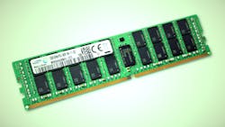
DRAM is not to be outdone, but it is trailing in stack size. Samsung’s latest 128-Gbyte DDR4 memory (see photo) uses a four-level stack. Many multilayer memory devices employ a bonded stack where each chip is wired to the base in the same fashion that a single die is wired. This requires that connectivity be done at the edge of the chips. Newer devices, including Samsung’s DRAM, employ through-silicon vias (TSVs). This is comparable to through-holes in a printed circuit board (PCB). It has multiple advantages, including the ability to place holes almost anywhere on the die. Samsung’s roadmap has eight- and 16-layer devices on it.
The number of layers varies with each type of device because there are other issues than just 3D stack connectivity involved in the design process. For example, DRAM operates at faster speeds than flash memory.
Still, there are more advantages driving the migration to higher stacks, including power savings and increased bandwidth. The trend toward massive in-memory databases is pushing capacities on the server side, while more compact platforms are pushing the technology in the embedded space.
There may be a limit to the number of layers that are practical, but for now we have not reached that limit.

This file type includes high resolution graphics and schematics when applicable.
About the Author
William Wong Blog
Senior Content Director
Bill's latest articles are listed on this author page, William G. Wong.
The latest blogs have been moved to alt.embedded on Electronic Design.
Bill Wong covers Digital, Embedded, Systems and Software topics at Electronic Design. He writes a number of columns, including Lab Bench and alt.embedded, plus Bill's Workbench hands-on column. Bill is a Georgia Tech alumni with a B.S in Electrical Engineering and a master's degree in computer science for Rutgers, The State University of New Jersey.
He has written a dozen books and was the first Director of PC Labs at PC Magazine. He has worked in the computer and publication industry for almost 40 years and has been with Electronic Design since 2000. He helps run the Mercer Science and Engineering Fair in Mercer County, NJ.
- Check out more articles by Bill Wong on Electronic Design
- Bill Wong on Facebook
- @AltEmbedded on Twitter
Comment About the Article
To join the conversation, and become an exclusive member of Electronic Design, create an account today!

Leaders relevant to this article: