1.2-V VIO SPI NOR Flash Reduces Overall System Cost and Power

What you’ll learn:
- Design compromises required for interfacing sub-10-nm SoCs with traditional 1.8-V SPI NOR flash.
- How a dual-voltage SPI NOR architecture can reduce BOM and simplify PCB layout.
- The effect of using a 1.8-V core supply with a dedicated 1.2-V I/O interface on read power, page programming speed, and data throughput.
Today’s emerging market segments embedded in edge AI, automotive, clean energy, and connectivity utilize system-on-chips (SoCs) built on fabrication process nodes of 10 nm and below.
Advanced SoCs operate at voltages from 1.2 V or even lower. Supporting higher-voltage I/O structure like 1.8 V, which is used with many NOR flash devices, can increase the SoC die size and make it more expensive. Using a NOR flash device with a 1.2-V voltage input/output (VIO) feature helps reduce cost as well as power consumption.
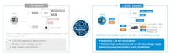
Traditional external flash memory devices support product portfolios that operate with 3.3- or 1.8-V power supplies. These devices can support high-speed read, fast program, and fast erase performance operations. Utilizing these devices with a 1.2-V SoC requires external level shifters or an SoC with such support built in. The alternative is to have the flash device interface with the SoC at 1.2 V while operating at a core voltage of 1.8 V and the power-management IC (PMIC) providing two voltages (Fig. 1).
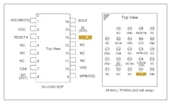
A typical example has 1.8- and 1.2-V power supplied to the VCC and VCC_IO pins (Fig. 2). The CC_IO pin is an additional pinout as a 1.2-V power-supply voltage to the I/O pins.
Today, two types of products support the 1.2-V SPI NOR flash architecture. One is the pure 1.2-V SPI NOR flash that supports 1.2 V for both power supply and IOs; and the other combines 1.8-V core voltage with 1.2-V VIO interface voltage.
Pure 1.2-V NOR flash faces the design challenge of delivering the full performance of 1.8-V devices. It operates at the lower 1.2-V core where internal flash read, program, and erase operations require intrinsic elevated charge voltage greater than the core voltage. This solution can support the low to median performance applications, but it may not be able to handle other higher-performance applications that need a two-voltage solution.
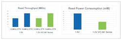
The two-voltage VIO solution saves a significant amount of power (Fig. 3).
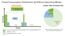
Overall power usage can be reduced using power-down modes of GigaDevice’s GD25NE SPI NOR flash chip (Fig. 4). Current draw drops to 12 µA in standby mode and 200 nA in deep power-down mode. The 256-byte page program time of 0.15 ms is around 40% faster than conventional 1.8-V SPI NOR flash devices.
About the Author
Conrado Canio
Director Technical Marketing, Flash BU, GigaDevice Semiconductor Inc.
Conrado Canio has been in the semiconductor industry for last 27 years with emphasis in Product Marketing (Flash Memory and Microcontroller Products), New Product Definition/Development, Business Development, Embedded System Design (Hardware and Software Integration), Semiconductor Testing/Debugging, and Supply Chain.
He worked at various companies including Silicon Storage Technology Inc., Microchip Technology Inc., Winbond Electronics, and lastly GigaDevice Semiconductor USA Inc. for over three years.
Conrado has overall expertise in the flash-memory market from managing new products and customers to handling product management/promotion/sampling/technical support to meet customers time-to-market, achieving up to $100M+ in revenue stream with strategic customers.
Comment About the Article
To join the conversation, and become an exclusive member of Electronic Design, create an account today!

Leaders relevant to this article: