What’s the Difference Between JESD230G and Earlier JEDEC Standards?

What you’ll learn:
- The key technical differences between JESD230G and earlier revisions of the NAND Flash Interoperability Standard.
- How the new Separate Command Address (SCA) Protocol improves performance by eliminating legacy bottlenecks.
- Why JESD230G impacts not just NAND devices, but also memory controllers, firmware, and SoC designs.
- How next-generation NAND flash systems will benefit a wide range of applications from consumer electronics to high-performance computing.
JEDEC is a global leader in developing standards for the microelectronics industry. JESD230 is JEDEC’s NAND Flash Interface Interoperability Standard. The first version of this standard, which was introduced in 2011, supported only 133 megatransfers per second (MT/s).
The latest revision to the JEDEC standard, JESD230 NAND Flash Interoperability Standard, introduces significant advances that pave the way for the next generation of NAND flash storage devices and systems that can support up to 4.8 gigatransfers per second (GT/s).
Such innovations will profoundly impact future NAND flash memories, necessitating changes to the raw NAND die, memory controllers, and firmware in the host system. The result will be a dramatic improvement in the performance of NAND-based storage devices and systems.
These changes will affect everything from consumer-level devices, e.g., smartphones and tablet computers, to enterprise-level installations that include data centers and cloud storage facilities. In addition, computationally intensive and data-intensive applications that will benefit from these changes include artificial intelligence (AI) and high-performance computing (HPC).
Who are the JESD230 Players?
Many groups of people influence and/or are affected (either directly or indirectly) by the JESD230 standard. A high-level visualization of these groups is shown in Figure 1.
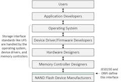
In the context of this article, the interface of interest is located between the raw NAND die and the devices that control them.
The Open NAND Flash Interface (ONFI) is an industry workgroup that develops open standards for NAND flash memory devices and the devices that communicate with them. ONFI seeks to standardize the low-level interface to raw NAND flash chips, thereby enabling interoperability between NAND devices and host controllers.
Meanwhile, the JESD230 standard defines the electrical, logical, and protocol-level interface between the controller and the raw NAND flash devices. These two organizations work closely together. In fact, in JEDEC, the NAND Flash Task Group is regarded as a Joint Task Group between JEDEC and ONFI.
>>Check out this TechXchange for similar articles and videos

How Does JESD230G Differ from Previous JESD230 Versions?
The pin names and functions in the JESD230 series of standards remained largely consistent from the original JESD230 through to JESD230F. Most changes during these revisions focused on performance improvements, power management, and feature enhancements, while maintaining backward compatibility, particularly in terms of pin functionality.
The pins and functions associated with standards JESD230 through to JESD230F may be referred to as the Conventional protocol (Fig. 2).
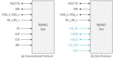
Note that multiple NAND die may be presented in the same chip package. From a high-level view, how does NAND flash work? The memory usually has a byte-wide data bus (other widths are sometimes employed). Inside the die, the memory is partitioned into “pages.” There may be tens of thousands of these pages, each containing tens of thousands of bytes. NAND flash memories are written to and read from one page at a time.
Writing to, or reading from, the device involves a sequence of actions, starting with a command byte (such as read, write, or erase), followed by a multi-byte address, which can be thought of as specifying the start of the page. The command and address are followed by a stream of data bytes being read from, or written to, the device.
In the case of the Conventional protocol, the low-speed command and address bytes, along with the high-speed data bytes, are all transferred on the same 8-bit bus (pins DQ[7:0]).
The problem is that the command and address transfer times haven’t kept up with the increasing data-transfer rates. This results in commands and addresses forming a bottleneck in the process.
To address this problem, the JESD230G standard has introduced the Separate Command Address (SCA) protocol. This separates the command/address (CA) and data buses, allowing for concurrent CA and data traffic, thus improving NAND interface efficiency. The pins associated with the SCA protocol are highlighted in blue in Figure 2b.
Observe the SCA pin. The packages of existing NAND flash chips include several NC (“not connected”) and NU (“not used”) pins. In the case of new JESD230G-compliant NAND flash chips, one of the NU pins is now employed as an SCA mode pin.
On power-up, this pin instructs the NAND to either act as a legacy device using the Conventional protocol, in which case the CE, ALE, CLE, and WE pins will behave as usual, or to use the new SCA protocol. This will cause the CE, ALE, CLE, and WE pins to be renamed and perform CA_CE, CA[1:0], and CA_CLK functionality, respectively. In this case, commands and addresses will be communicated as a series of 2-bit fields via the CA[1:0] pins. As a result, these transfers will occur concurrently with data transfers on the DQ[7:0] pins.
Conclusion: JESD230G Support
Now that the new JESD230G standard has been formally ratified, leading NAND flash manufacturers, such as KIOXIA, are developing next-generation devices that support this standard.
At the same time, electronic design automation (EDA) vendors like Cadence and Synopsys are developing new NAND flash controller IP cores for use in system-on-chip (SoC) devices. Similarly, top vendors of standalone NAND flash memory controller integrated circuits (ICs), e.g., Hyperstone, Marvell Technology, Phison Electronics, and Silicon Motion, are developing new controllers for use in next-generation systems.
The users of these systems, along with the software developers who create applications to run on them, will enjoy the performance benefits of these new NAND flash technologies while remaining unaware of the changes taking place “under the hood.”
By comparison, hardware designers and software developers in charge of creating these next-generation systems need to be aware of what’s “coming down the pike” with respect to JESD230G-enabled NAND flash memory devices and controllers.
>>Check out this TechXchange for similar articles and videos
About the Author

Doug Wong
Senior Member, KIOXIA Technical Staff
Doug Wong is a Senior Member of the Technical Staff at KIOXIA America, where he has contributed to the advancement of memory technologies since 1993. He began his career with KIOXIA in the company’s Memory Division (then part of Toshiba America) and has since focused on a broad range of memory solutions, including PSRAM, SRAM, MROM, EPROMs, NOR flash, and NAND flash.
Doug has been an active contributor to industry standards as a member of the JEDEC JC42.4 committee since 1996. He holds a Bachelor of Science in Electrical Engineering from California Polytechnic State University San Luis Obispo and a Master of Science in Electrical Engineering, with a focus on solid-state physics, from UCLA.
Comment About the Article
To join the conversation, and become an exclusive member of Electronic Design, create an account today!

Leaders relevant to this article: