Securing ReRAM
Check out more TechXchange Talks videos.
Crossbar's latest resistive RAM (ReRAM) technology can be used to implement physically unclonable functions (PUFs). ReRAM has garnered interest as an embedded non-volatile memory (NVM) that scales better than flash memory. Flash storage becomes challenging below 28 nm, which typically keeps it out of processor designs that are implemented using the newest silicon process nodes below 10 nm.
I talked with Ashish Pancholy, VP Marketing and Sales at Crossbar, about the company's technology and new announcement in the video (above). Crossbar's filamentary-based ReRAM makes implementation possible in high-retention and high-density versions, and it provides multiple-time programming (typical R/W memory), few-time programming (FTP, unique to ReRAM at this time), and one-time programming (OTP).
Links
Transcript
Wong: Non-volatile memory is extremely important these days, regardless of what platform you're doing or working with. It could be in microcontrollers all the way up to the cloud, but there are a number of different technologies out there. Resistive RAM or ReRAM is one of those and Crossbar is a company that is actually doing quite a bit in this area.
So Ashish, could you tell us a little bit about ReRAM technology and how yours works?
Pancholy: Absolutely. Well, let's start off by saying that Crossbar’s ReRAM technology is a different flavor from other technologies that might also be considered to be ReRAM, Resistive RAM, technologies.
And one of the differences is that Crossbar’s technology is a filamentary ReRAM technology. In other words, there's a filament that's created or not, between two electrodes that enables a digital one versus a digital zero.
So the way it works is what you're seeing on the left side of this picture (Fig. 1). Here is a rendition of what comes out of a silicon fabricated, manufactured state of the ReRAM and what you see is the labels there. The TE is the top electrode the BE is the bottom electrode and in between as a switching medium, kind of like a dielectric, and with the top electrode has atoms in order to write the cell to its other state.
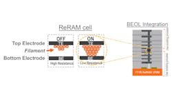
So when it comes out, there's a high resistance between the top and bottom electrodes because of the switching medium, which is kind of like a dielectric.
And in order to turn that state to a lower resistant state, what we have to do is to is to apply it potentially between the top and bottom electrodes and what the potential losses is to two things.
Number one, it ionizes the atoms in the top electrode and then the electric field that is caused because of that potential causes the ions to kind of move down from the top to the bottom electrode.
So what happens is as you continue down this process, what you see is eventually you'll get to a state which is shown on the right side of the top picture. Now you see these metallic atoms or ions forming a filament between the top and the bottom electrodes. Because of this, the resistance in the state goes from a high resistance to a low resistance.
Essentially what we've done in this in this process is we've programed cell from a high to a low resistance. So these are the two resistance states of out of our storage element for the filamentary ReRAM.
Wong: Okay. So what does this do with respect to the manufacturing process, scalability? Where are ReRAM cells being placed?
Pancholy: Yeah, so that's a really good question. So let's start with the last question first.
Where are the cells being placed?
What you see on the right side of the screen (Fig. 1) is essentially a cartoon showing a seamless process. At the bottom with the green is the baseline seamless process where the transistors exist and then the darkish layers that you see on top are depicting metal layers.
So you can see that the ReRAM cell is being placed in between layers of metal. In this particular instance, it's between layers of metal, one to three, between four and five layers of metal. Practically, you could place it wherever it's convenient for the end user.
What's some of the performance and CMOS manufacturing details?
It uses standard CMOS manufacturing. There's no special material or elementor process required for this. The technology is extremely scalable and the reason for that is that if you look at one of the key characteristics of this of this technology. A metric of this technology is the on-off ratio, which is the ratio of the resistance in the off-state versus the on-state.
If you look at that as a multiple or a ratio, what is that number? That number is high. It's in the thousands, maybe ten tens of thousands.
So what happens is, if you can picture this, the top and bottom electrons, the off -state of this memory cell is essentially a function of the cross-sectional area of the top and bottom electrode.
As we squeeze that area down, everything else being the same, the resistance between the top and the bottom electrodes is going to grow and it's going to grow as a square of the dimension that the top and bottom electrodes have in that process.
So think of this as in the off-state. The resistance between the top and bottom electrodes is growing as you scale down the process in the on state.
What's happening is we've created a metal filament between the top and bottom electrodes, and independent of the geometry of the node, to a first order, the dimensions of that filament remain the same so that resistance remains the same as we scale down. But the off-stage resistance is shrinking as a square of the dimension.
So if you put the two together, the On-Off ratio is actually getting far superior to everything else being the same as we scale down the geometry node.
Since it's not a charge-based storage at all, unlike incumbent technologies like flash (memory), we don't have to worry about this technology.
Not much scaling.
Well, the filament itself is a sub-ten nanometer dimension filament, single digit nanometer. You don't need to worry about that scaling with the geometry node. In essence, the scalability in terms of performance, this is truly a randomly readable and writeable technology.
So in terms of just to get calibrated on the random read axis times, depending on the architecture and the requirements, the read access times could be well under 20 nanoseconds for a random read. The write performances does not require any block function. So you don't have to do a block erase, for instance with page arrays, before you write the contents that you need. You can just do them independently.
Wong: Okay. ReRAM also has essentially very long life and long retention, but there's also a high-speed version versus a high-density version that you have. How are those different and how are they implemented?
Pancholy: The high-speed version essentially has every ReRAM element is coupled with a select transistor to enable access to the ReRAM element somewhat along the lines of a different technology that has an access transistor for every capacitive storage element.
That particular configuration of having a cell with its on select transistor enables high speed transactions in read and write. On the other hand, if you're focusing purely on the density and maybe making a trade off at access times, then we have another flavor of our technology where with a single transistor we can essentially access multiple cells and the multiple cells could be in the thousands.
This is enabled with Crossbar's proprietary selector device that is built within an ReRAM stack. We have an ReRAM stack (Fig. 1) along with a selector device that is not shown here for that flavor of technology. That selector device ensures that a single transistor can reliably access large swaths of ReRAM elements. That enables us is to provide a far superior density.
At the same time, it enables multiple stacks of ReRAM being enabled in the different layers of metal. So now you can have a three-dimensional multiples of ReRAM cells between the two layers.
Wong: Okay. Now, there's a note here about scalability below 28 nanometers. Why is that significant? Does it have anything to do with flash (memory)?
Pancholy: Yeah, it has. It has a lot to do with flash and the reason it significant is that flash, as we all know, is a charge-based or charge-storage based technology.
There's a charge that's captured could be between floating gates or it could be other mechanisms like SONOS (silicon-oxdide-nitride-oxide-silicon), but essentially it's based on how much charge you can store. With that charge, the smaller the node the smaller the amount of charge that you have access to. At some point you just run out of enough charge to reliably hold onto the memory storage.
So typically the 28-nanometer node, or it may be the two X nanometer node, where flash becomes extremely unreliable for most applications.
That's why technologies, like Crossbar’s filamentary ReRAM, are targeting that space really well with all the performances that they can sustain and support.
Wong: Excellent. Now let's get to the more interesting things in terms of new stuff that you're working on. This is with respect to security and part of that is there are multiple ways to look at storage. There is multiple time (MTP) writes that typically DRAM and everybody else has. There is OTP, which is one-time programing, and there's something in between called FTP.
Could you tell us a little bit about what you're doing with ReRAM and also get into a little bit of details on the security aspects?
Pancholy: Absolutely. Security is a very, very big thing given the market conditions today and a lot of our customers are extremely sensitive to the security aspects behind memory. Security is key for communication systems, for other systems, storage devices, etc., both in light of reliability as well as in light of malicious attacks that are occurring on an increasing basis.
So just to give you a calibration there are tens of billions of interconnected IoT devices with 50 plus million attacks on them growing at a clip of 50% a year. So it's a big problem for everyone.
One of the aspects that we can address with Crossbar’s filamentary ReRAM technology is that inherently the technology, with refined algorithms, can serve as an MTP which means that you can program and erase multiple times, thousands of times. With the right algorithm it is only enabled to be programed once for security reasons.
So the Crossbar technology filamentary ReRAM technology enables both MTP operations and OTP for secure purposes. There's something in the middle where, perhaps because of certain key applications, you want to enable only a few time programable (FTP) capability. So, for instance, maybe ten times or so and then no more.
The fundamental ReRAM technology that Crossbar has done enables all flavors of these MTP, OTP and FTP based on the same fundamental process technology using algorithms.
Wong: You can dynamically adjust that, can't you?
Pancholy: We can absolutely dynamically adjust that because the base technology is the same way that we're not changing the process. All we are doing is we are using different algorithms to enable this kind of performance.
Wong: Now that's just with the read/write approach. You've also talked about PUF for example, getting really down and dirty in terms of preventing access or unwanted access to data.
Pancholy: Absolutely. So PUF, a Physical Unclonable Function, serves as a unique identifier or a digital fingerprint. So a PUF is an element that's going to be different from day to day, even for a device that are manufactured on the same process, the same line, maybe even the same wafer, definitely within the same wafer (Fig. 2).

So it serves as a digital fingerprint. It's useful for authentication, knowing when a device is truly what its saying it is and then it's used for crypto as the basis of certain cryptographic functions that are important for secure communications, for secure storage, etc. So that's the that's the importance of a PUF.
So what Crossbar technology is enabling the same basic ReRAM technology that is used for storage and memory is now also available for PUF applications.
It's not just another technology. We find it's far superior to incumbent technologies for applications and the reasons for that are as follows.
The first one is that it's physically more random than other PUF approaches and I'm talking about hardware plus approaches. One of the incumbent technologies is SRAM-based. SRAM-based PUF are essentially based on micro fabrication type variation die-to-die that cause events SRAMs to come up in a certain state versus other states or cells going to seemingly randomly between zero and one states.
For ReRAM the randomness that we get when we program a ReRAM comes from essentially a stochastic or quantum stochastic process of where the filament is going to form.
So it's far more random. It's not based on any micro fabrication type basis. It comes from an inherently quantum stochastic process. So it's more random.
We run this test. We run several tests to make sure that we understand the performance and that's the basis for the higher degree of performance that we found.
The second thing is that the fact that we can embed a ReRAM onto an SoC on the same technology because now we can have a ReRAM memory coexist with a revamped PUF on the same piece of silicon.
The attack surface is hugely reduced for a hacker and what I mean by that is that if you have a separate PUF from an SoC, then there's a lot of exposure in terms of wires and pins in a system that can easily be attacked by a hacker who is just hellbent on figuring out your contents.
So we are dramatically reducing the attack surface by having everything embedded on the same die.
The third point here is that we have a reliable PUF for the very low bitrate. What I mean by that is, if you have an SRAM-based PUF, as an example, the means of generating the randomness is to turn it off and then turn it on and then some cells will fall into one state and some others into the other state, seemingly random.
The point is if you were to do it multiple times, what is the likelihood that you'll get the same state as you did the previous time? That's very key for certain applications and in essence, typically that error rate of what happens the second time or third time or fourth time when you generate the same key is what your attempt is that you'll get an error rate that could be in the percents, could be the single digit percents, it could even be in the tens of percents for a reason.
We have multiple ways of implementing with PUF Crossbar filamentary ReRAM technology. We find is that a revamped error rate for the same kind of test is in the PMM (part/million) and maybe on occasions when we've had virtually zero errors when we generate keys multiple times using the same structure.
That's a huge advantage in terms of having a little bit error rate.
Jumping to another kind of related point here is what the higher bit error rate in some incumbent technologies leads to is in order to minimize there's certain applications that just cannot tolerate having errors. Period. Not even a single bit.
In order to accomplish that level of reliability, there is use of helper data that comes from the from a server. For instance, to help make sure that it's, like an ECC correction, to make sure that the data is correct. It's reliable. It's the same every single time from a PUF
For an invasive attack this opens up the means of attacking, maybe using the helper data to figure out what the content might be over prolonged usage that is eliminated with a view. So that's a huge advantage.
We find that the PUF based on the ReRAM is unclonable. We talked about this based on a stochastic process., the filament is a creation is based on an atomic level, stochastic process, and it's secure.
And the security comes from, not just the fact that, that there are certain inherent aspects of the ReRAM that make it hard to decipher or to infer the content stored in a ReRAM cell. I'll come to that in just a second.
In terms of invasive attacks, if someone is hellbent on trying to do that, that means they have to access the data inside. So there are several ways in which the ReRAM is more resistant to invasive attacks, and that's the that we'll talk about in just a little bit.
There's an environmental aspect of it behind the PUF. If you know how long can the data be held for, number one, and then, in the event that you actually want to cut your losses, let's say the specific secret code is in the hands of a hacker, and you already know that. Maybe you just want to destroy the data
and cut your losses. An ReRAM-based PUF enables you to do that unlike some other technologies.
So you can wipe out the contents of the PUF pretty easily at low power and then here's the beauty having done that or maybe even without having done that, if you'd like to create a new set of secret keys using the same means that you use, which is a ReRAM based PUF. You can actually do that and you can be assured it'll be a different set of keys than what you've created before.
So that's extremely useful as well in certain applications and, then finally, the last point here would be that the technology scales to advance nodes, and it can be there's memory technology coupled with PUF technology, coupled with OTP, MTP, FTP, all variants of the memory technology that provide for very, very finely tuned suite of storage and have been able to secure applications.
Wong: Excellent. Well, has anybody tried to attack this yet?
Pancholy: Yes, indeed. In fact, what we at Crossbar did was we had a lot of data because we've been curious about our own technology.
We do know that some of the more benign ways of attacking and trying to infer first stored content deal with some of these aspects (Fig. 3). So starting at the top here, power analysis. There are ways that you can essentially sniff out the power, how much power you're consuming, what's your cycle rate? What's your clock frequency? Maybe you can infer some something about the content stored in the memory when it reads and writes.

There are optical attacks as well. You can use laser malicious laser type attacks to to maybe inject faults in your memory, and then you might be able to infer something about the power used or what happens electrically as a signature to what's with the content is stored on your memory.
Then there are transistor, number three here on the list. Transistor based technologies are also susceptible to photo emission analysis like electron hole recombination. It results in photonic emission that can be picked up with sophisticated equipment.
The extremely motivated and sophisticated hacker can piece things together to infer the contents of your memory based on photonic analysis.
So in the case of Crossbar ReRAM technology, there is no photonic emission because there's there are no transistors in terms of storage. The data is stored in metallic filaments so there's no related photonic emission from them. They are completely immune to that.
The next thing is transmission electron microscopy and advanced techniques like that.
Once again, they cannot look at micron level defects in the structure of the ReRAM because these are atomic level defects that will cause the filament to be in a certain place versus another place within the top and bottom electrode kind of space. That's a really, really hard, virtually impossible to use TEM optics are microscopy to gather where the filament might be or might not be because you just don't know where to look for it. So you don't know if you haven't found it or if it doesn't exist, which are the two states of the cell.
With electromagnetic analysis the cell density is so high that you just cannot find enough probes to be able to infer the content, If you want to use this devious mechanism to maybe infer or makes some inference about your data content stored in a ReRAM.
Also, if you take it one more level because of the fact that a ReRAM is created in between layers of metal in a seamless process, you can very easily create a Faraday cage based on those metal layers and build a protection around that that will then inhibit any EM-type radiation in the right band so that you are completely immune to EM-type sniffing potentially trying to infer what the data stored is.
Finally, like I talked about before, the low bit error rate associated with the ReRAM PUF is virtually zero unlike incumbent technologies like an SRAM-based PUF you can find single digit, maybe even tens of percents of bitrate over the lifetime of the product.
Back to your question about what we are doing next or what we have done next. We're excited about sharing this with everyone is that in addition to some of the methods I just described regarding malicious hacking and trying to infer the contents of either the memory or the PUF, both of which could be danger for certain applications. Those are electrical and electromagnetic in nature. Maybe you're trying to induce some faults with a laser nondestructive and then imaging using multiple means.
We actually went beyond that and we hired a third party based out of New Mexico and gave them the explicit challenge of using any means and all means available to them, including destructive to use all the equipment (Fig. 4). These guys have been in the business. They have 25 years in reverse engineering and have access to sophisticated semiconductor equipment.

The challenge was to infer the contents of data that were stored in a ReRAM array.
The bottom line after the exercise concluded was that they couldn't infer the contents of our ReRAM.
So that was yet another positive in this in this quest
Wong: Well, great. Well, thank you for filling us in on the technology behind ReRAM as well as the new security support that crossbar is providing.
Pancholy: Thank you. My pleasure.
About the Author

William G. Wong
Senior Content Director - Electronic Design and Microwaves & RF
I am Editor of Electronic Design focusing on embedded, software, and systems. As Senior Content Director, I also manage Microwaves & RF and I work with a great team of editors to provide engineers, programmers, developers and technical managers with interesting and useful articles and videos on a regular basis. Check out our free newsletters to see the latest content.
You can send press releases for new products for possible coverage on the website. I am also interested in receiving contributed articles for publishing on our website. Use our template and send to me along with a signed release form.
Check out my blog, AltEmbedded on Electronic Design, as well as his latest articles on this site that are listed below.
You can visit my social media via these links:
- AltEmbedded on Electronic Design
- Bill Wong on Facebook
- @AltEmbedded on Twitter
- Bill Wong on LinkedIn
I earned a Bachelor of Electrical Engineering at the Georgia Institute of Technology and a Masters in Computer Science from Rutgers University. I still do a bit of programming using everything from C and C++ to Rust and Ada/SPARK. I do a bit of PHP programming for Drupal websites. I have posted a few Drupal modules.
I still get a hand on software and electronic hardware. Some of this can be found on our Kit Close-Up video series. You can also see me on many of our TechXchange Talk videos. I am interested in a range of projects from robotics to artificial intelligence.