Research Program Seeks Advances in Wide-Bandgap Power Semiconductors

The projects in ARPA-E's SWITCHES—short for “Strategies for Wide-Bandgap, Inexpensive Transistors for Controlling High-Efficiency Systems”—program focus on developing next-generation power switching devices. Such devices could dramatically improve energy efficiency in a wide range of applications, including new lighting technologies, computer power supplies, industrial motor drives, and automobiles.
The SWITCHES program is one of ARPA-E’s Open Funding Opportunity Announcements (Open FOAs). It sought transformational advances in wide-bandgap (WBG) materials, fabrication, and device architectures. ARPA-E’s goal in this program is to foster development of high-voltage (1200 V+), high-current (100 A), single-die power semiconductors. Upon ultimately reaching scale, they would have the potential to achieve functional cost parity with silicon power transistors while also offering breakthrough circuit performance.
SWITCHES projects aim to find innovative new WBG semiconductor materials, device architectures, and device-fabrication processes that will enable increased switching frequency, enhanced temperature control, and reduced power losses—all at substantially lower cost relative to today's solutions. More specifically, SWITCHES projects are tasked with advancing bulk gallium-nitride (GaN) power semiconductor devices, the manufacture of silicon-carbide (SiC) devices using a foundry model, and the design of synthetic diamond-based transistors.
Leveraging WBG Semis
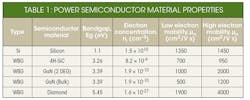
Development of WBG power semiconductors has opened the door to improved power switches. Table 1 compares several different WBG device materials relative to Si. WBG semiconductors are capable of low-loss operation at high voltages (>1 kV to tens of kV), high frequencies (tens of kHz to tens of GHz), and high temperatures (>150°C).
Power converters based on WBG devices can achieve higher efficiency as well as higher gravimetric and volumetric power-conversion densities. For example, in a recent demonstration, a 2-kW motor driven by high-frequency GaN devices increased efficiency by over 2% at full load and 8% at low load relative to the same motor being driven by Si IGBTs.
It’s possible that WBGs could eventually achieve functional cost parity with silicon power transistors. In addition, when compared with silicon power transistors, WBGs exhibit improved performance in terms of lower losses, higher switching frequencies, and higher temperature operation. By achieving these cost and performance characteristics, WBGs would reduce the barriers to being widely deployed in stationary and transportation energy applications.
Recent research results indicate that new materials advances, device architectures, and device fabrication processes could substantially accelerate progress toward WBG devices that achieve both higher current ratings and functional cost parity with silicon-based devices. So far, these approaches have received relatively little attention because they are perceived to be high risk and technically unproven.
Still, several classes of technological and scientific challenges must be solved to achieve high-voltage, high-current WBG power semiconductors, on a pathway to widespread adoption as power switches.
In particular, fabrication processes require numerous improvements:
• Fabricating buried p-type layers or improvements in metal-semiconductor contact formation on N-polar or semi-polar GaN crystal orientations.
• Device designs compatible with lower-cost fabrications processes, like those that allow use of legacy silicon device-fabrication facilities.
• Device structures that minimize mask count, which would reduce costs.
• Device structures that reduce thermal management challenges.
• Relatively thick films of high quality (low defect) WBG materials.
New approaches to growing WBG materials at higher speeds are needed, too, including:
• New substrate crystal growth.
• New wafering and fabrication processes.
• Bulk GaN substrates with high-quality material, required for many vertical device concepts, are currently limited to small sizes and costly production.
• High-quality bulk GaN substrates with low defect densities are critical, as it has been shown that thermal conductivity of GaN strongly depends on material quality.
• New chemistries for epitaxial growth or substrate refining techniques appear to have substantial potential. Many substrates have small domain structures unsuitable for large-area power devices.
• New approaches to fabricating bulk substrates could be an important pathway to achieving high-current low-cost devices.
• The III-V photovoltaics community has demonstrated how epitaxial liftoff and substrate reuse can be used to achieve substantially lower-cost devices despite high substrate costs. These same concepts might find application in WBG power semiconductors.
Technical Areas of Interest
ARPA-E is most focused on applications that provide a well-justified, realistic potential of meeting or exceeding all of its Primary and Secondary Technical Targets. The following technical areas are of particular interest:
• WBG power semiconductors utilizing novel fabrication processes or device structures not previously supported by ARPA-E, other governmental agencies, or previously developed for commercial application; such technologies might include vertical GaN device structures.
• Approaches to device fabrication that are compatible with substrate reuse (i.e., device liftoff), and novel structures compatible with much-lower-cost fabrication processes and high die current ratings.
• New approaches to fast, high-quality thick-film epitaxial growth that enables rapid fabrication of high-voltage devices.
• Investigation of technologies with the potential to enable extremely low-cost and highly scalable free-standing wide-bandgap substrate fabrication. Such technologies might include, but are not limited to, new GaN, ZnO, SnO2, sapphire, or other wide-bandgap substrate growth techniques.
• Approaches that enable larger substrate sizes and substantially reduced defect densities. These may include advances in new chemistries for epitaxial growth or substrate refining techniques.
Researchers who might be working on subsystem materials or component-level innovations are highly encouraged to partner with device designers and manufacturers as a means of evaluating device-level functionality resulting from breakthroughs in the proposed effort.
Technical Performance Targets
The vision for ubiquitous WBG power semiconductor device deployment hinges on these devices reaching functional cost parity with today’s dominant power semiconductor switch technology in high-power applications.
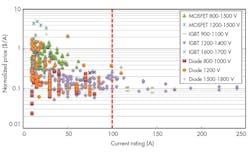
Figure 1 plots the price ($/A) of existing high-voltage silicon power semiconductor devices using data from electronic components distributor Digi-Key as of late May 2013, and those pricing trends continue today. Variability in this plot is associated primarily with different package technologies and the different applications targeted by each particular device.
The plot indicates that 1200-V, 100-A devices are typically priced between $0.10/A and $0.20/A today. Si device costs are expected to continue to fall incrementally over the next decade. Based on these data, it is expected that WBG devices achieving costs of below $0.10/A would represent a functionally cost equivalent technology, with potential advantages of WBG devices.
The superior performance of WBG devices, relative to the Si switches they are replacing, will allow them to gain adoption in many applications before reaching functional cost parity. However, truly widespread adoption in high-power, conservative, cost-conscious applications such as industrial motors and automotive applications may require functional cost parity for the devices themselves.
Applicants must justify how the proposed technology holds promise to meet ARPA-E’s $0.10/A device cost target. The cost target is intended to be a forward-looking consideration of device costs, including packaging, assuming successful technology development and subsequent scaling of manufacturing for ubiquitous deployment.
For example, applicants should describe all assumptions related to the scale that would be needed to achieve $0.10/A. In addition, ARPA-E expects selected applicants will revise cost-models through the course of the proposed effort. They would reflect technical advances achieved during the work and demonstrate how increased scientific understanding provides a pathway to ultimately reaching cost targets in the program.
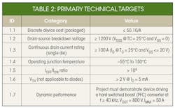
In Table 2, Primary Technical Targets 1.2 – 1.6 describe device characteristics that should be demonstrated experimentally in a single device by the end of the project period. These targets are consistent with the characteristics of devices required in high-power applications, including many motor drive systems and in electric vehicles. Primary Technical Target 1.7 is a requirement to demonstrate that devices designed and fabricated under this program are suitable for high-frequency switching applications. Appropriate thermal management of devices will be critical to successfully meeting this technical target. Devices achieving all of the primary technical targets will be relevant for a wide range of applications.
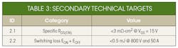
Secondary Technical Targets listed in Table 3 are based on the desire to achieve low losses and high switching speeds. The targets are based on an assumed cooling limit of approximately 200 W/cm2 under 40-kHz hard switching with a 50% duty cycle. This cooling limit is consistent with the capabilities of commonly used low-cost packaging technologies.
ARPA-E Proposals
ARPA-E does not accept unsolicited proposals. Instead, ARPA-E broadly solicits energy-related research proposals using periodic Open FOAs. Open FOAs are generally issued every two to three years. In addition, ARPA-E accepts, on a rolling basis, proposals to the Innovative Development In Energy-Related Applied Science (IDEAS) Funding Opportunity Announcement for single-phase efforts of up to 12 months and up to $500,000.
Once projects have been selected, ARPA-E FOAs are no longer open for applications. The projects in SWITCHES (https://arpa-e.energy.gov/?q=arpa-e-programs/switches) are final. To avoid confusion, ARPA-E hosts an Open FOA every few years (2009, 2012, 2015), in which applicants make tackle a much broader set of energy and technology challenges. While SWITCHES was open to anyone interested in applying, it is not an "Open FOA" in the ARPA-E parlance.
To receive announcements about ARPA-E’s new Open FOAs and other program-specific FOAs, join its newsletter mailing list, available here. More information on the IDEAS FOA is available here. Do not contact ARPA-E about unsolicited proposals.
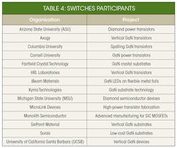
A number of SWITCHES projects are small businesses being funded through ARPA-E's Small Business Innovation Research (SBIR) and Small Business Technology Transfer (STTR) program. Participants of the SWITCHES program are listed in Table 4.
About the Author

Sam Davis
Sam Davis was the editor-in-chief of Power Electronics Technology magazine and website that is now part of Electronic Design. He has 18 years experience in electronic engineering design and management, six years in public relations and 25 years as a trade press editor. He holds a BSEE from Case-Western Reserve University, and did graduate work at the same school and UCLA. Sam was the editor for PCIM, the predecessor to Power Electronics Technology, from 1984 to 2004. His engineering experience includes circuit and system design for Litton Systems, Bunker-Ramo, Rocketdyne, and Clevite Corporation.. Design tasks included analog circuits, display systems, power supplies, underwater ordnance systems, and test systems. He also served as a program manager for a Litton Systems Navy program.
Sam is the author of Computer Data Displays, a book published by Prentice-Hall in the U.S. and Japan in 1969. He is also a recipient of the Jesse Neal Award for trade press editorial excellence, and has one patent for naval ship construction that simplifies electronic system integration.
You can also check out his Power Electronics blog.
Comment About the Article
To join the conversation, and become an exclusive member of Electronic Design, create an account today!

Leaders relevant to this article: