Use a Prototyping Kit to Simplify Energy Harvesting Designs
Before working with a design, it may not be obvious exactly how much power an energy harvesting circuit will be able to provide given the conditions of its environment. This influences the required size and quality of the energy harvesting source and energy storage. To further complicate the design, considerations such as energy storage leakage, regulator power loss, load average/peak power, transducer max power point regulation, and battery capacity can have a significant impact on the system’s reliability. These issues must be addressed and tested in a real-world environment to accurately understand whether a system will work reliably out in the field.
At the start of an energy harvesting circuit design, two frequently asked questions are:
- How do I efficiently convert my transducer’s high-impedance output into a regulated power supply?
- Given my size and ambient energy availability constraints, is it possible to meet my load requirements using power from an energy harvesting source?
A variety of energy harvesting switching regulators can efficiently convert a high-impedance transducer’s output into a regulated supply (Fig. 1). An important feature of these ICs is their ability to regulate the output of an energy harvesting transducer to a particular operating point regardless of how much power is pulled from the device. This feature is used to keep the transducer operating at its maximum power point (MPP) so that the regulated output has the highest power capability possible for the chosen transducer in the given ambient conditions.
1. This energy harvesting switching regulator is powered by a high-impedance source meeting load requirements.
When designing an energy harvesting circuit, it is necessary to minimize the amount of power consumed by the load while maximizing the amount of energy extracted from the transducer. Under normal operating conditions, the average power available to the system must be greater than the average power used by the system. Furthermore, the system must be able to survive load transients. So, in addition to the average power condition being met, the system must also have enough energy storage to provide the maximum burst of energy required by the load while still maintaining a reasonably regulated power supply. This energy storage is generally employed through the use of a bank of capacitors, a supercapacitor, or a battery.
Ambient Energy
Another challenge of energy harvesting circuit design is that ambient energy is often not a reliable or consistent source of power (Fig. 2). In a solar-powered system, for example, about half of a daylight cycle offers little or no energy. Also, clouds passing over a solar panel are not predictable and can cause a significant loss in available energy. In cases like these, the energy storage capability of a capacitor may not suffice.
To combat long periods of energy unavailability, it may be necessary to rely on the long-term energy storage of a battery. Energy harvesting circuits that include a battery have the added benefits of load transient handling and instant power-up.
However, using a battery often decreases the amount of time that the system can remain in the field without maintenance; primary (non-rechargeable) batteries will eventually need to be replaced and secondary (rechargeable) batteries will deteriorate in health over time. Several energy harvesting switching regulators use batteries to back up the energy harvesting source during periods where the ambient energy alone is not enough to support the load.
2. Terrestrial solar panel irradiance (partly cloudy) is shown.
Energy Harvesting Prototyping
The Gleanergy energy harvesting wireless sensor node development platform is a fully-customizable kit that allows users to prototype many varieties of energy harvesting (EH) wireless sensor node (WSN) solutions. The kit is broken into several parts:
- DC2344A Multi-Source Energy Harvesting Demo Board with Battery Chargers and Life-Extenders
- DC2321A Energy Harvesting Application Demo Board with E-Ink Display
- DC2510A Shield Board for Use with DC2321A Dust Demo Board
- DC2274A-A SmartMesh IP USB Network Manager
Designers can configure the kit to accept a veriety of unique energy harvesting sources, write a custom program on the LTP5901-IPM Dust mote assemble their own sensor circuit on the shield board, and communicate with the SmartMesh manager over the wireless network. The LTP5901 is a printed circuit board assembly (PCBA) product with on-board chip antenna in the Eterna family of IEEE 802.15.4e solutions. It features a highly integrated, low-power radio design as well as an ARM Cortex-M3 32-bit microprocessor running SmartMesh IP embedded networking software. The LTP5901-IPM, at 24 mm × 42 mm, is built for surface-mount assembly.
The DC2344A handles all the energy harvesting aspects of the kit and is used to power the rest of the application. The board hosts two types of energy harvesting transducers (thermoelectric generator and solar cells) and a terminal block for connecting a piezoelectric transducer or any other high-impedance AC source. In addition to the provided sources, input turrets allow the user to connect external transducers to the board.
As a backup power supply, the board holds a primary and a secondary battery which can be easily routed to any of the appropriate ICs. On-board energy storage is also available in the form of a supercapacitor or a bank of ceramic capacitors.
Low-Power Wireless Sensor
The DC2321A is a wireless sensor node equipped with an E-ink display for user feedback. The system is capable of monitoring and managing its available energy, logging information from sensors, and sharing this data over a wireless network.
When connected to DC2344A for power, the DC2321A board monitors the status outputs of all the on-board energy harvesting ICs. Two coulomb counters on the DC2321A allow the processor to monitor the energy output of these batteries, which will vary depending on the amount of energy which can be harvested from the system’s surroundings.
Data acquisition and general operation is controlled by the LTP5901-IPM, a wireless sensor node, or mote. This module is integrated with Dust Networks’ low-power radio design, as well as an ARM Cortex-M3 32-bit microprocessor which is embedded with SmartMesh IP networking software, allowing it to form a reliable network with other motes in even the harshest of environments.
The GUI which supports the DC2321A displays all of the data monitored by the mote in a user-friendly way that consumes much less energy than an update to the E-ink display. In addition, long-term data logging is supported, and the gathered data can be exported to a comma-separated value (CSV) file for review in Excel. The GUI can also be used for changing network settings.
Sensor Prototyping Board
The DC2510A is a shield board for use with the DC2321A Dust application demo board. This board is designed to allow users to build their own custom application circuits directly on the DC2321A with access to all pins of the LTP5901-IPM Dust mote. The board offers footprints of common sensor and IC packages, as well as prototyping space for routing.
ADI’s low-power sensors are a great fit for energy harvesting circuits. Demonstration circuits and firmware are available using the following products:
- ADXL362 Micropower 3-Axis Digital Output MEMS Accelerometer
- ADT75 ±1⁰C Accurate 12-Bit Digital Temperature Sensor
- ADPD2214 Low Noise, High Sensitivity Optical Sensor
SmartMesh Manager USB Dongle
The DC2274A-A serves as a network manager for a SmartMesh IP wireless sensor network. With its compact USB dongle form factor, the DC2274A-A, along with SmartMesh IP wireless nodes, makes it easy to rapidly deploy a wireless mesh network for field trials and to accelerate sensor product development.
The USB dongle connects to a computer’s USB port and allows for a user interface to monitor data being transmitted wirelessly. The SmartMesh Python GUI examples can be used to send and receive raw data between the manager and a remote DC2321A connected to the same mesh network. The SmartMesh SDK can also be used as a template for creating custom Python GUIs specific to any application.
Prototyping with the Gleanergy Kit
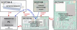
With all pieces of the Gleanergy kit combined, a complete energy harvesting wireless sensor node is formed. The boards can then be configured to convert the system into a custom solution:
The DC2344A can be configured to work with the user’s transducer; custom batteries, capacitor energy storage, and regulation settings are also chosen. The DC2510A can be populated with a sensor specific to the user’s application and the DC2321A can be programmed with custom application code to read from this sensor and transmit data over the network. Network data is monitored by the USB manager plugged into a computer, and this data is then displayed on a user’s custom Python GUI built from the SmartMesh library.
3. The Gleanergy kit interconnectivity and data flow diagram is shown.
The Gleanergy kit’s demonstration program provides examples of all of these features, so the user only needs to tweak the existing hardware and firmware in order to create their own system (Fig. 3). Once all of these steps are completed, the prototyping phase is finished. All that remains is to strip away the parts of the kit that are not needed and create a final energy harvesting wireless sensor node system design from the components used during prototyping.
As a result, prototyping with the Gleanergy kit offers the following benefits:
- Demonstrates energy harvesting circuits. Educates users unfamiliar with energy harvesting by showing how a complete system can work. Demo manuals and datasheets offer additional detailed information.
- Speeds up prototyping. Demonstrates a complete solution, allows integration of custom transducers and components, and gives demonstration code that can be modified into a final solution, GUI allows real-time monitoring of the system for testing. Includes a prototyping board for out-of-the-box configuration.
- Minimizes prototyping costs. Offers all components of the system in one kit so that they do not need to be purchased separately.
Design Example
The following demonstrates some of the tools and example designs available for learning how to use the kit to create a custom application.
This application is based off of the ADT75 ±1⁰C Accurate 12-Bit Digital Temperature Sensor. This sensor, along with a few others, is compatible with a DC2321A sensor firmware demo and a Python GUI specifically made to demonstrate the usage of the kit with custom sensors.
1. Mount the Sensor onto DC2510A
The ADT75 can be mounted directly onto one of the SOIC footprints on the DC2510A. With the IC soldered, the rest of the pins can be routed to the headers according to the DC2321A header pinout.
2. Reprogram DC2321A with the ADI Sensor Demo Firmware
Using a JTAG debugger or Eterna Serial Programmer (ESP), load the ADI Sensor Demo firmware onto DC2321A. Source code and programming instructions are available at the GitHub address below.
3. Run the Python GUI and Monitor the Sensor Data
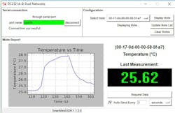
Connect the DC2274A-A Network Manager into a USB port on the computer and run the Python GUI. From the GUI, temperature data can be requested at a configurable interval. When the data is received over the network, it is plotted on a graph (Fig. 4) that shows a fingertip being placed on the ADT75 and then being removed.
Source code and Python GUI usage instructions are available online.
4. The DC2321A Python GUI displays and plots the wireless sensor node temperature data.
The example firmware and GUI code can easily be tweaked to work with any sensor attached to a DC2510A.
Through these design examples and the other features of the kit, users can familiarize themselves with energy harvesting while minimizing prototyping time and cost.
About the Author
Voice Your Opinion!
To join the conversation, and become an exclusive member of Electronic Design, create an account today!

Leaders relevant to this article:


