Power Limits Make Hot Swapping More Robust
Hot swapping, the act of inserting and removing circuit boards into an active backplane has been used in telecom servers, USB interfaces, firewire interfaces and CompactPCI applications.[1] By keeping the system backplane voltage live, faulty boards can be removed and replaced with new boards, but still keep the system live for other boards in the system. In general, an external FET is used with a hot-swap controller to control the inrush currents. But not all hot-swap controllers are created equal.
Using some hot-swap controllers to control inrush currents can make hot swapping into a live backplane unreliable. The capacitors on the circuit boards provide a low-impedance path for the supply, causing large inrush currents. The inrush currents can cause damage to board capacitors, trace lines and connectors. The system voltage can drop below the system-reset threshold due to the inrush currents and cause other boards connected to the backplane to reset.
This scenario can be reliably averted by picking a controller that combines both programmable power and current limiting. In turn, this allows you to maintain a margin of safety to the safe-operating-area (SOA) boundary for reliable protection without the need to oversize the external FET.
Hot-swap controllers are designed to limit the inrush current by controlling an external FET. The controllers also limit the current during fault conditions when the output shorts out to ground or there are large load transients.
One can assume that picking a FET that can withstand the dc current load and maximum input voltage would be sufficient. However, controllers that only have the ability to control the current cannot guarantee the FET will stay within the SOA under all operating conditions.
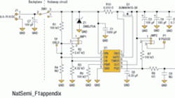
There are controllers that can provide both power-limit and current-limit control. One such example is National Semiconductor's LM5069 IC (Fig. 1). The inrush current is sensed across the sensing resistor (RSENSE). The controller will only allow a maximum voltage across RSENSE. If the voltage increases beyond the maximum voltage, the controller will modulate the gate voltage to keep the current at a maximum level, the current-limit mode.
The maximum power across the FET is programmed through the PWR pin. If at any time the power across the FET (VDS × ILIMIT) is greater than the programmed power limit, then the ILIMIT is reduced such that the FET power is equal to the programmed power limit, the power-limit mode.
The maximum current (ILIMIT) will be maintained for a limited amount of time.
The maximum time allowed for the current limit is programmed through the timer pin by the fault-detection current, fault threshold and external capacitor. Once the timer reaches the fault threshold, the controller shuts off the gate and the output is disconnected from the system input voltage.
System undervoltage and overvoltage are detected through a resistor divider on the undervoltage lockout (UVLO) and overvoltage lockout (OVLO) pins, respectively. The part verifies that the input voltage is within a specific range, above the undervoltage threshold and below the overvoltage threshold. If the input voltage is out of range, then the gate shuts off. The power good pin (PGD) is an open drain output. When the output (VOUT) reaches the input (VIN) within 1.25 V, the open drain pull-down device is disabled and PGD is pulled up through the pull-up resistor to the VOUT rail. The PGD output can be used to flag downstream circuitry to indicate that the VOUT voltage is “good.”
When controlling the current during a hot-swap event or short-circuit fault condition, the external MOSFET must remain within the SOA to prevent FET failure. Fig. 2 shows Vishay's SUM40N15-38 FET SOA curve.[2] It has a maximum drain-to-source voltage (VDS) of 110 V, and at a low VDS, the current is limited due to the RDSON of the FET. The curves shown with time are the maximum energy limitations of the FET.
A horizontal line can be drawn on the SOA curve (the green line in Fig. 2) to indicate a controller with only current-limit control. During normal operation (i.e., VDS is low), the current is limited to 5 A and the FET is within the SOA boundaries. However, at a large VDS, the controller limits the current to 5 A and, depending on the programmed fault time, the FET may go outside the SOA. For example, if the system backplane voltage is 50 V, the current limit is set to 5 A and the programmed fault time is 40 ms, then a short circuit on the output would cause the FET to operate beyond the implied 40-ms SOA (the green dot in Fig. 2).
The red curve in Fig. 2 indicates the combination of both the current and power limiting of the LM5069 on the SOA curve. The programmed current limit is set to 5 A, and the power limit is set to 50 W. The fault time is again programmed to 40 ms.
When the 50-V output is shorted, the part will no longer operate in the current-limiting mode (5 A), but instead operates in the power-limiting mode (50 V × 1 A = 50 W). The FET will remain below the implied 40-ms SOA curve and prevent the FET from failing (the red dot in Fig. 2).
At a VDS < 10 V, the part goes into the current-limiting mode and provides the necessary current load to the output all the while keeping the FET inside the SOA. The LM5069 power-limit feature will only take control if the power across the FET tries to go beyond the programmed limit of 50 W. Otherwise, the current-limit feature controls the FET.
Bench Data
Application boards were made for both the LM5069 and current-limit controllers. The online version of this article shows their two test-board circuits, but their respective test results are shown here. Both parts had the condition of a 50-V input voltage, a 5-A current limit and a 40-ms fault time. The LM5069 had the added feature of a 50-W power limit. Both applications shorted the output via a load resistor causing the VDS to increase.
The oscilloscope plot for the controller with current limiting only is shown in Fig. 3, while a plot for the LM5069 is shown in Fig. 4. The output load increased the VDS to 30 V. Initially, the current is limited to 5 A, but after 10 ms the FET fails and the input voltage shorts to the output voltage. The input voltage craters and limits the current to the current limit of the voltage supply. The timer reaches the 40-ms timeout, but cannot shut off the gate since the FET is damaged.
Looking at the SOA curve, the FET can only withstand a 10-ms pulse at a VDS of 50 V and a drain-to-source current (IDS) of 5 A. Once the FET goes beyond 10 ms due to the current-limit control, the FET fails (the red dot in Fig. 5).
As shown in Fig. 4, the output loading increases VDS to 45 V, and the LM5069 limits the power across the FET to 50 W. Once the timer reaches the fault threshold, the part shuts off the FET. The LM5069 controls the FET well within the SOA curves in this shorted condition (the blue dot in Fig. 5).
Fig. 6 shows the condition of pure current limiting by the LM5069. The output loading caused the current to increase, but not so heavily as to cause an increase in VDS. The LM5069 limits the current to 5 A and the FET shuts off after the programmed fault time of 40 ms. Again, the LM5069 controls the FET inside the SOA (the green dot in Fig. 5).
References
-
Bearfield, Jonathan M., “Introduction to Hot Swap,” TechOnline, www.techonline.com, 2005.
-
Vishay SUMN40N15 data sheet, www.vishay.com.
-
National Semiconductor LM5069 data sheet, www.national.com.
Comment About the Article
To join the conversation, and become an exclusive member of Electronic Design, create an account today!

Leaders relevant to this article: