Feedback Circuit Improves Hysteretic Control
The hysteretic power supply is simpler than the voltage- or current-mode closed-loop-control dc-dc switchers, although its simplicity may be a bit deceiving due to component variations and potential sources of “injected” feedback voltage. Along with its simplicity, the hysteretic power supply is popular today for its low cost, inherently stable operation (with no need to perform loop analysis), extremely fast load response time that requires no compensation, and suitability for applications requiring low dropout because the main switch is a p-channel power MOSFET that can be driven up to 100% duty cycle.
The hysteretic controller IC is the key element in the conventional hysteretic power supply. And, even better results are possible with a simple modification to the conventional hysteretic controller IC circuit. That modification requires only the addition of a single capacitor and resistor in the feedback circuit of the controller IC. To describe the modification, we will first look at the performance of the conventional hysteretic controller.
Principles of Operation
As shown in Fig. 1, at the heart of the hysteretic controller IC is a comparator with a small amount of voltage hysteresis (VHYS). When the comparator feedback voltage exceeds the internal reference voltage (VREF) plus its hysteresis, the comparator output turns off the main power switch. Then, when the feedback voltage drops below VREF minus VHYS , the power switch turns on and the cycle repeats itself. Thus, exceeding the hysteresis voltage determines the switching frequency and overall power-supply performance.
For predictable switching frequency operation within a desired range, the IC's comparator needs a reasonably clean and well-controlled triangular ramp voltage superimposed on the dc feedback voltage, which essentially matches the comparator's hysteresis. Unfortunately, this feedback signal can vary significantly due to the input-supply voltage, output capacitance (COUT), COUT equivalent series resistance (ESR), inductor value and board layout.
Board layout is critical with any switching supply, and this is perhaps even more important with hysteretic controllers due to high sensitivity to ground and voltage feedback noise that can directly affect switching frequency. Careful adherence to recommended board layout is essential to avoid drastically varying operating frequencies that may result in excessive output-voltage ripple and poor regulation. Additionally, variations in external components, especially COUT and its ESR, can cause large shifts in operating frequency. Fortunately, there are some techniques that can circumvent these pitfalls.
Referring to Fig. 1, a typical hysteretic buck controller IC includes a comparator, PMOS driver, one-shot, short-circuit protection and inrush control, and does not require an oscillator to control the switching frequency. The one-shot limits the duty cycle and external component power dissipation during an overcurrent event. Basic operation requires feedback ripple voltage (Fig. 2) to be compared with an internal VREF (1.242 V) to toggle the high-side PMOS driver whenever the comparator threshold exceeds its 10-mV hysteresis. The conventional hysteretic controller generates this ripple voltage by using the inductor ripple current conducting through COUT and some amount of ESR.
Common methods to create ripple voltage in Fig. 2 include:
-
Rely on ESR inherent in COUT.
-
Insert an external ESR in series with COUT that is sufficiently larger.
-
Insert a known series resistor between COUT and inductor.
Determining Switching Frequency
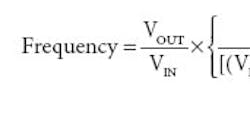
The drawback to using only the ESR of COUT is that its value is not well controlled and may vary significantly. Adding a series resistor to COUT adds to VOUT ripple, and inserting it between COUT and inductor reduces efficiency. Furthermore, low resistance values (e.g., 100 mΩ) add cost. When using any of the previously mentioned methods, the feed-forward capacitor (CFF) is recommended to reduce output ripple voltage by providing an ac-coupling path from VOUT to the feedback pin. This reduces VOUT ripple required by the controller because feedback resistors R1 and R2 will not divide the output ripple voltage down. Eq. 1 estimates the switching frequency for methods 1, 2 and 3:
where α equals (R1+R2)/R1 and equals 1 when using CFF, TD equals the approximate comparator delay of 110 ns and L equals the inductor inductance (henries).
Several factors determine the switching frequency in Eq. 1. For example, COUT and its ESR are dominant factors that impact the switching frequency. Changes in COUT from part to part, COUT trace inductance or additional capacitance at the point of load alter the effective ESR. Calculations based on Eq. 1 are rough estimations, and design engineers must also empirically determine circuit operation with a known set of components, board layout and operating conditions. The problem is that all variations are not easily accounted for during testing. The design challenge is not just multiple variables, but sensitivity to variable tolerances.
Fortunately, a new design approach can improve switching frequency operation and take much of the guesswork and unpredictability out of designing a hysteretic switching regulator. Instead of using the net output ripple voltage created in the final output capacitor, use the source that produces ripple voltage beforehand. In a sense, we can use an “emulated” output ripple voltage by taking the voltage swings from the switch node that produces the same triangular ramp required for operation as shown in Fig. 2. The buck regulator circuit in Fig. 3 uses the LM3485 hysteretic controller and highlights the components in red that emulate VOUT ripple voltage.
Instead of relying on output ripple voltage at C2 and feeding this back to the comparator, the switch node voltage creates a current source. During the on time of Q1, a constant current of (VIN - VOUT)/RS charges CFF, and during Q1 off time, CFF ramps down from the current sink of approximately VOUT/RS to produce the required ramp signal based on I = Cdv/dt. Choose capacitor CFF so its impedance is much less than feedback resistor R1 at the desired switching frequency. Capacitor CS serves as an ac coupling path and its size is approximately 20 times the value of CFF. Note that Eq. 2 no longer includes the output ESR or inductor value, and is derived by analyzing the integration components and comparator at a given duty cycle (D) determined by VIN and VOUT. Rearranging this equation and solving for RS in Eq. 3 helps to set the desired frequency using RS as a dependent variable:
An example using an LM3485 evaluation board will help solidify the design process and operating performance. Measurements in Table 1 were done using an unmodified board (Fig. 3 without CS or RS and with CFF = 100 pF). The VIN range was chosen to be 8 V to 16 V, VOUT equals 3.3 V and output load equals 10 Ω. The output load has a negligible effect on the switching frequency, provided the circuit maintains the continuous mode. If IOUT is less than one-half the inductor ripple current, the discontinuous mode will cause the frequency to reduce as required.
Another benefit of the LM3485-type controller is that under light loads, very low regulator quiescent current is achievable since the p-channel MOSFET only switches when necessary without the need for a charge pump or boot-strap circuit.
With this design, no additional ESR other than that inherent in C2 (COUT) is used to set the switching frequency. Although frequency deviation with respect to VIN is acceptable, it is important to emphasize that very wide variations will occur from board to board mainly because of variations in the COUT ESR and inductor tolerance. For example, if COUT is a Sanyo 6TPC100M 100 µF with a rated ESR of 45 mΩ at 100 kHz, then from Eq. 1 the calculated frequency is 376 kHz, where α equals 1, ESR equals 45 mΩ, VHYS equals 10.5 mV, TD equals 110 ns, L equals 22 µH, VIN equals 13.7 V and VOUT equals 3.3 V.
The measured frequency is actually 160 kHz because COUT ESR is much lower than rated and it varies with temperature, further widening the frequency spread. Table 1 shows the variation in switching frequency for input voltages from 8 V to 16 V. Here, the frequency deviation percentage is relative to 160 kHz.
Emulated Ripple Voltage Example
Next, we modified the same board to include emulated ripple voltage circuitry with CFF, CS and RS as shown in Fig. 3. For example, calculated values of CFF, CS and RS are for the desired switching frequency of approximately 330 kHz, and measurements were taken to confirm the results.
For the design procedure:
-
Set CFF-based feedback resistor R1 (33 kΩ) to be << impedance at 330 kHz.
-
Select CFF equals 2.2 nF for an impedance of 1/(2 π FC) = 219 Ω.
-
CS equals approximately 10 to 20 times CFF , so choose 68 nF, which is not critical.
-
Duty cycle can be calculated based on a volts-seconds balance across the inductor for on and off cycles (measured at 26% for nominal VIN of 13.7 V and VOUT of 3.3 V).
-
Calculate required RS for desired frequency using VHYS equals 10.5 mV and TD equals 110 ns, from the LM3485 data sheet using Eq. 3.
Note that a TD of 110 ns is primarily the propagation delay of the LM3485 comparator. For a larger input capacitance of the selected MOSFET, between 10 ns to 20 ns may need to be added:
RS = 287 kΩ.
As shown in Table 2, test results of the same evaluation board, but with modified circuitry, came very close to what was expected, using RS equals 287 kΩ, CS equals 68 nF and CFF equals 2.2 nF.
In this design, the COUT ESR does not appreciably impact the switching frequency. Actually, we don't require this type of capacitor when using the emulated ripple voltage method, and a smaller and less-expensive ceramic capacitor with very low ESR between 10 µF to 22 µF is preferable. Note that if an output capacitor with too large an ESR is selected, it will tend to increase the frequency from the summation of emulated and feedback ripple voltage.
Table 2 shows the variation in switching frequency for input voltages from 8 V to 16 V. The frequency deviation percentage is relative to 340 kHz.
PC-Board Design
Board layout is a separate topic, but it is critical to achieving desirable operation of the hysteretic controller, so a few points should be emphasized:
-
Make the feedback trace thin and keep it well away from the inductor and high di/dt traces of the input and switch node.
-
Place the feedback resistors very close to the controller.
-
Connect the feedback network ground directly to the controller ground pin and run the controller signal ground path completely separate from the power ground return to the input source ground.
-
Connect C1 (CIN) and its ground as close as possible to the anode side of D1 to contain the high di/dt loop. For additional points, the LM3485 evaluation board (AN-1227) serves as an excellent example of proper layout.
The most important objectives are to quantify and narrow the switching frequency variations that can occur due to component characteristics as well as board layout. Compared with previous methods of creating feedback ripple voltage, the emulated approach provides a much-improved method to initially set frequency, and removes the two largest variables (COUT ESR and inductance) from the equation. Better control of the frequency improves overall system cost and reliability. This occurs because you do not have to size the design for a relatively low frequency; therefore, the inductor does not require as high of a peak current rating, and it allows for the optimization of input and output capacitors.
About the Author
Comment About the Article
To join the conversation, and become an exclusive member of Electronic Design, create an account today!

Leaders relevant to this article: