Advanced Module Architecture Satisfies Medium-Power Requirements
A new IGBT module features an advanced concept based on bipolar level shifters. As a result, the integrated silicon-on-insulator (SOI) driver is immune to changes in referential voltage, thus providing a high level of reliability in applications with an output power of up to 15 kW. For low-power applications (i.e., for motor outputs below 2 kW), integrated modules have gained acceptance over the past decade, largely driving out discrete solutions. In this power range, the generic term intelligent power module (IPM) refers to three-phase inverter circuits with integrated drivers that are soldered onto a lead frame and packaged using transfer mold processes.
For higher power applications, the heat dissipation properties must be increased, which is difficult to achieve in these package types. IPMs developed especially for higher power applications are based on drivers mounted on a conventional circuit board integrated into classical modules. However, these modules require complex internal connection technology and also must manage the problem of providing sufficient cooling for the driver components.
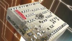
For medium-power applications (i.e., for motor outputs of 2 kW to 15 kW), converter-inverter-brake (CIB) modules have gained a solid footing over the past few years. CIBs are efficient solutions that combine all of the power switches with high cooling requirements in one single module case. Semikron MiniSKiiP modules have been particularly successful for use in CIB solutions, because they combine a user-friendly assembly concept with advanced packaging technology.
Conventional packaging technology used in power modules employs solid copper plates that function as base plates for the entire module's components. These base plates are normally 23 mm thick and involve a number of problems.1 Different thermal expansion coefficients of the base plate and the ceramic power substrate affect performance.
Composite boards made of copper/ceramics/copper — referred to as direct bonded copper, owing to the manufacturing process — causes considerable stresses in the solder layer after soldering, resulting in strong bending in the overall system. The bending produces hollows in the assembly level, which fulfills an important thermal function in the module. A suitable base plate design can help reduce such hollows; however, due to the viscoplastic properties of the solder, a time-dependent relaxation will occur that alters the bending. Therefore, an optimum base plate shape for any given point in time cannot be defined.
More than 10 years ago, these considerations led to the development of packaging solutions without a base plate. In such solutions, both the solder layer and the base plate itself are no longer in the thermal path to the heat sink. If a suitable pressure system is used to provide a small-sized gap between the base of the substrate and the heat sink, the disadvantages caused by the lack of thermal spreading in the base plate can be virtually compensated for by reducing the thickness of the thermal paste layer.
SPRING CONTACTS
The technology used for the module connections characterizes user-friendly module assembly. The MiniSKiiP modules use spring contact technology for the load and control contacts. This provides two user benefits:
- No additional assembly equipment is needed to connect the module to the PCB. The PCB is simply placed between the module and the pressure lid. The thermal contact and all electrical connections are created in a single step when the module is mounted onto the heat sink.
- Disassembly is possible at any given time, which boosts the service friendliness of this technology. Unlike solder connections with through-hole technology, spring contact technology also simplifies PCB layout.
Additionally, use of spring contacts provides an advantage for module design. Implementation of spring contacts enhances design flexibility, meaning the contacts can be positioned relatively freely on the DBC. This enables the development engineer to position the contacts to ensure that the CIB has optimum dynamic electrical properties. The number of internal connections can be reduced, thus increasing overall reliability. As stated previously, spring contact technology allows for flexible module design. With different configurations of springs in the implemented shafts inside the module case, different variations easily can be achieved within the same module family.
In the MiniSKiiP IPM, the positions of the spring contacts can be adapted to implement the necessary load and control contacts (Fig. 1). An edge seal, which is pressed into the upper of the PCB during assembly, surrounds groups of spring contacts of the same potential range as well as the entire contact area, thus increasing the degree of protection from ambient influences.
The current carrying capacity of this spring is 20 A for continuous duty and is limited by Joule's law of electric heating. In a MiniSKiiP IPM, the load contacts are all formed by three parallel springs, allowing for an effective continuous current of 60 A.
While the advantages of spring contacts are relatively broadly recognized, some reservations exist with regard to long-term reliability under the extreme conditions that are not uncommon in power electronic applications. These reservations are fueled by negative experiences with plug-in connectors, which can cause problems with small currents and voltages.
The spring contacts used in MiniSKiiP modules, in contrast, are very different from standard commercial plug connectors and provide a far higher contact force in the bargain. With standard plug contacts, contact force is limited because too high a contact force causes the forces needed to plug and unplug the connector to increase. The typical contact pressure in plug connectors is in the 10 N/mm2 range.
With MiniSKiiP spring contacts, the conditions are very different, because the contact force comes from the screw that presses the module onto the heat sink during assembly. During this assembly, a pressure in the range of 20 N/mm2 to 100 N/mm2 is established in the contact interfaces of the springs. The typical screw connection between a load connection in a traditional module and a dc link bus bar achieves a pressure of around 50 N/mm2. Therefore, a spring contact is more comparable to a screw connection than to conventional plug connectors.2
For contact forces of between 4 N and 6 N (Newtons) per spring, as is the case in MiniSKiiP, Ag is used as preferred contact plating. Extensive long-term investigations have confirmed this contact surface has a high degree of reliability and is suitable for PCBs with an SnPb surface, as well as for RoHS-compliant chemistry, Sn, hot-air leveling (HAL) Sn and Ni/Au-flash (ENIG) surfaces. The only PCB surface finish not recommended for use with spring contacts is organic surface protection (OSP).
SOI DRIVERS
A MiniSKiiP with a high-voltage integrated circuit (HVIC) is known as a CIB IPM module. Advantages of CIB IPM modules include increased integration density and user-friendliness.
The HVIC platform used here is 600-V SOI foundry technology. The advantage of SOI technology over pn-insulated concepts is the comparatively small leakage currents. Furthermore, the dielectric insulation of all the active components guarantees immunity from the latch-up effect, which in pn-insulated HVICs can lead to malfunction and ultimately destroy the inverter. Finally, SOI technology allows the HVIC to be used up to a maximum operating temperature of 200°C, making this technology suitable to handle future operating temperature requirements in power modules.
The HVIC works at a supply voltage of between 12 V and 17 V, and controls three TOP and three BOT switches with paired interlocking to prevent simultaneous turn-on. A fourth BOT switch is for use in a brake-chopper or PFC circuit. The inputs are compatible with TTL or 3.3-V CMOS logic, and the signal run time between inputs and outputs is approximately 300 ns. An error management function processes internal errors (voltage undersupply) and external errors (e.g., overcurrent detection) and ensures all the CIB switches are turned off.
A fundamental characteristic of the SOI driver is an advanced level shifter concept that is largely immune to variations in driver reference voltage. In an inverter, steep current slopes occur during load current switching that, together with the parasitic inductances present in the system, generate voltages between the emitter potential of the IGBT and the reference voltage of the driver. These voltages can have both polarities. Depending on the polarity, the voltage between gate and emitter is either increased or reduced. This leads to a change in switching properties and, in unfavorable conditions, can result in undesired turn-on or turn-off of the switch. In a worst-case scenario, it can result in inverter destruction. Additionally, the use of shunts to monitor the current results in a load-dependent voltage shift between driver reference voltage and IGBT emitter, which can lead to similar problems.
In low-power IPMs, these parasitic voltage fluctuations are normally very low; however, they increase as the power increases, meaning that as the current increases the impact of this effect also becomes more serious. For this reason, an advanced level shifter concept was developed that allows compensation of voltage variations in both polarities for BOT and TOP switches.
The basic principle concept of the BOT level shifter is shown in Fig. 2a. One TOP and one BOT level shifter are driven on two independent transmission channels. The level shifters are conventional static CMOS level shifters with additional diodes in each path. Depending on the polarity of the voltage shift between primary and secondary side, either the TOP or the BOT level shifter is used for signal conversion, while the other level shifter is inactivated by the blocking diodes. On the secondary side, just a simple OR circuit is needed.
The realization of the level shifter for the TOP switch (Fig. 2b) is more complicated, as no p-MOS transistors are available for blocking voltages of 600 V. For this reason, pulse signal conversion based on high-voltage nDMOS and high-blocking diodes is used. The pulsed conversion allows for the reduction of transverse currents and thus switching losses.
This advanced concept for bipolar level shifters in TOP and BOT control makes the driver immune to variations in reference potential, which are only limited by the blocking capability of the level shifter switches. The function of the level shifters in the case of static voltage changes is demonstrated by the signal characteristics in Figs. 3a and 3b for a voltage change of +20 V and -20 V, respectively. Dynamic voltage variations also are easily compensated, as shown in Fig.4a. Here, the characteristic of the drive signals on the secondary side is virtually ideal, despite the fact that a noise signal was introduced in between the emitter voltage and driver reference voltage.
Fig. 4b shows a photo of an SOI driver layout indicating the individual channels. The high-blocking DMOS transistors and diodes for the bipolar level shifters of the TOP switches can also be seen.
MiniSKiiP IPM WITH INTEGRATED SOI DRIVER
The HVIC is mounted directly onto the DBC of the CIB power module. This achieves short signal paths and thus low parasitic properties in the drive paths (Fig. 5).
The DBC comprises 0.2-mm-thick copper layers with a 0.3-mm thick Al2O3 ceramic layer on both sides. Conducting traces and insulation trenches of 0.4 mm each is necessary for distributing the driver control signals.
The first step in the assembly process is to solder the power components and temperature sensor. HVIC and SMD gate resistors are then integrated using conductive adhesive. The upper contacts of the power components are connected using 300-µm-thick aluminum wire bonds, while the driver is connected using 50-µm aluminum wire bonds. The circuit then is encased with silicon soft mold and the substrate inserted into the module case, into which the contact springs have already been assembly. The module assembly is complete once the soft mold has been cured.
A significant advantage of the direct driver assembly on the DBC is the good heat dissipation. In fact, a thermal resistance of around 4 K/W can be achieved for the approximately 4.9-mm × 3.1-mm driver chip. In a conventional SOP28 case, in contrast, the thermal resistance of a chip with approximately the same dimensions is approximately 75 K/W. The low thermal resistance allows for far higher power in the driver output stages. While the first prototypes had an output current of 500 mA for an output voltage of 15 V, the output current of the next generation can be doubled, resulting in better chip control in medium-power applications.
REFERENCES
-
Scheuermann, U.; Beckedahl, P. “The Road to the Next Generation Power Module — 100% Solder Free Design,” Proc. CIPS 2008, ETG-Fachbericht 111, 111-120, Nürnberg, 2008.
-
Lang, F.; Scheuermann, U. “Reliability of Spring Pressure Contacts under Environmental Stress,” Microelectronics Reliability 47 (2007), 1761-1766.
-
Vogler, B.; Roβberg, M.; Herzer, R; Reuβer, L; and Wurm, T. “600 V Converter/Inverter/Brake (CIB) — Module with integrated SOI Gate Driver IC for Medium-Power Applications,” Proc. CIPS 2008, ETG-Fachbericht 111, 261-265, Nürnberg, 2008.
About the Author
Scheuermann
U.
Comment About the Article
To join the conversation, and become an exclusive member of Electronic Design, create an account today!

Leaders relevant to this article: