Flyback Controller IC Integrates Power Factor Correction
Linear Technology Corporation’s LT3798 is an isolated flyback controller with single stage active power factor correction (PFC). Efficiencies greater than 86% can be achieved with output power levels up to 100W. Depending on the choice of external components, it can operate over a 90VAC to 277VAC input range, and can easily be scaled higher or lower. Furthermore, the LT3798 can be designed into high input voltage DC applications, making it suited for industrial, EV/EHV automotive, mining and medical applications.
Fig. 1 shows a typical application for the LT3798. Table 1 lists the key functions of device pins that control LT3798 operation. This IC is a current mode switching controller intended specifically for generating a constant current/constant voltage supply with an isolated flyback topology. To maintain regulation, this topology usually uses output voltage and current feedback from the isolated secondary side of the output transformer to VIN. Typically, this requires an opto-isolator. Instead, the LT3798 uses the external MOSFETs peak current derived from a sense resistor to determine the flyback converter’s output current, without requiring an opto-coupler.
As shown in Fig. 1, the output transformer has three windings, including the output. The external MOSFET’s drain connects to one of the primary windings. The transformer’s third winding senses the output voltage and also supplies power for steady-state operation. The VIN pin supplies power to an internal LDO that generates 10V at the INTVCC pin. Internal control circuitry consists of two error amplifiers, minimum circuit, multiplier, transmission gate, current comparator, low output current oscillator and master latch. Also, a sample-and-hold circuit monitors the third winding’s output voltage. A comparator detects the discontinuous conduction mode (DCM) with a capacitor and series resistor connected to the third winding.
During a typical cycle, the gate driver turns on the external MOSFET so that a current flows in the primary winding. This current increases at a rate proportional to the input voltage and inversely proportional to the transformer’s magnetizing inductance. The control loop determines the maximum current and a comparator turns off the switch when it reaches that current. When the switch turns off, the energy in the transformer flows out the secondary winding through the output diode, D1. This current decreases at a rate proportional to the output voltage. When the current decreases to zero, the output diode turns off and voltage across the secondary winding starts to oscillate from the parasitic capacitance and the magnetizing inductance of the transformer.
All windings have the same voltage across them, so the third winding rings too. The capacitor connected to the DCM pin trips the comparator, which serves as a dv/dt detector, when ringing occurs. This timing information is used to calculate the output current. The dv/dt detector waits for the ringing waveform to reach its minimum value and then the switch turns on. This switching behavior is similar to zero volt switching and minimizes the amount of energy lost when the switch is turned on, improving efficiency as much as 5%. This IC operates on the edge of continuous and discontinuous conduction modes, which is called the critical conduction mode (or boundary conduction mode). Critical conduction mode operation, enables use of a smaller transformer than continuous conduction mode designs.
Power Factor Correction
The LT3798’s VIN_SENSE pin connects to a resistor divider from the supply voltage. The lower of the two error amplifier outputs is multiplied with the VIN_SENSE pin voltage. If the LT3798 is configured with a fast control loop, slower changes from the VIN_SENSE pin would not interfere with the current limit or the output current. The COMP+ pin would adjust to the changes of the VIN_SENSE. The only way for the multiplier to function is to set the control loop to be an order of magnitude slower than the fundamental frequency of the VIN_SENSE signal. Operating offline, the fundamental frequency of the supply voltage is 120Hz so the control loop unity gain frequency needs to be set less than approximately 12Hz. Without a large amount of energy storage on the secondary side, the output current will be affected by the supply voltage changes, but the DC component of the output current will be accurate.
An internal multiplier enables the LT3798 to achieve high power factor and low harmonic content by making the peak current of the main power switch proportional to the line voltage. A power factor greater than 0.97 is achievable for most applications. For an explanation of power factor correction, see the sidebar “Why Correct Power Factor”?
Starting Up
This IC uses a hysteretic start-up to operate from high offline voltages. A resistor connected to the supply voltage protects the IC from high voltages. This resistor is connected to the VIN pin and bypassed with a capacitor. When the resistor charges the VIN pin to a turn-on voltage set with the EN/UVLO resistor divider and the INTVCC pin is at its regulation point, the IC begins to switch. The resistor cannot provide power for the IC in steady state, but relies on the capacitor to start-up the IC, then the third winding begins to provide power to the VIN pin along with the resistor. An internal voltage clamp attached to the VIN pin prevents the resistor current from allowing VIN to go above the absolute maximum voltage of the pin. The internal clamp is set at 40V and is capable of 20mA (typical) at room temperature. Ideally, the resistor connected between the input supply and the VIN pin should be chosen so that the internal clamp shunts less than 10 mA.
Transformer specification and design is a critical part of successfully applying the LT3798. Because the current on the transformerís secondary is inferred by the current sampled on the primary, the transformer turns ratio must be tightly controlled to ensure a consistent output current. A turns ratio tolerance of ±5% from transformer- to- transformer could result in an output regulation variation more than ±5%. Fortunately, most magnetic component manufacturers can guarantee a turns ratio tolerance of ±1% or better. Several leading magnetic component manufacturers have produced pre-designed flyback transformers for use with the LT3798.
MOSFET and Diode Selection
With a 1.9A gate driver, the LT3798 can effectively drive most high voltage MOSFETs. A low QG MOSFET is recommended to maximize efficiency. In most applications, the RDS(ON) should be chosen to limit the MOSFETís temperature rise. The drain of the MOSFET is stressed to VOUT × NPS + VIN during the time the MOSFET is off and the secondary diode conducts current (NPS = Turns ratio from primary to secondary). But in most applications, the leakage inductance voltage spike exceeds this voltage. The voltage of this stress is determined by the switch voltage clamp. Make sure the switching waveform due to the leakage inductance voltage spike is below the MOSFET’s breakdown voltage. A transient voltage suppressor and diode are slower than the leakage inductance voltage spike, which would cause a higher voltage than expected.
The secondary diode stress may be as much as VOUT + 2×VIN/NPS due to the anode of the diode ringing with the secondary leakage inductance. An RC snubber in parallel with the diode eliminates this ringing, so that the reverse voltage stress is limited to VOUT + VIN/NPS. With a high NPS and output current greater than 3A, the IRMS through the diode can be very high, so select a low forward drop Schottky.
The LT3798 is available in a thermally enhanced 16-pin MSOP package. The LT3798E and LT3798I versions operate from -40°C to 125°C. The LT3798H is tested and guaranteed to operate from a -40°C to 150°C operating junction temperature.
Why Correct Power Factor?
A power supply’s power factor affects the harmonics that an AC-DC supply generates on the powerline. To understand the effect of power factor and harmonics, we first have to look at their effect on AC power distribution. Electric utilities have major difficulties when distributing power for loads that include AC-DC power supplies without power factor correction. These power supplies are nonlinear loads that:
- Distort the AC waveform.
- Cause harmonics currents that can impact operation of other equipment on the same utility line.
- Can cause fires, from neutral wires overheating.
- Can overstress and shorten the lives of power transformers.
- Can overload AC-power generators.
Starting In the 1980’s, the European Union decided to place the burden for solving these problems on the manufacturers of products employing AC-DC power supplies. Since then, it has undergone several revisions to set standards for limiting the amount of current products may draw at harmonics (integer multiples) of the powerline frequency. The LT3978 complies with power supplies rated up to 100W. Table 2 lists the equipment classifications of the IEC 61000-3-2 Standard for Harmonic Line Current Emissions.
In the U.S., there is the Energy Star program of the Environmental Protection Agency and Department of Energy that promotes use of energy efficient products and practices. Products that qualify with these requirements may display the Energy Star logo. Power supplies that meet Energy Star requirements must meet strict guidelines that specify efficiency and power factor (power factor value also affects harmonics). Table 3 lists the requirements for internal and external power supplies. Internal power supplies rated at less than 75 W must meet the minimum efficiency specified in Table 3. Internal supplies rated at ≥75 W must meet both the efficiency and minimum power factor requirements.
Power factor is relevant because typical AC-to-DC power converters load a powerline with a diode bridge driving a capacitor (Fig. 2). This load is nonlinear because two diodes of the bridge rectifier are in the direct power path for either the positive or negative half-cycle of the input ac line voltage. This type of load draws line current only during the peak of the sinusoidal line voltage, resulting in line current input peaks (Fig. 3) that cause power line harmonics. Line harmonics are comparable in magnitude to the fundamental harmonic current at line frequency. Fig. 4 shows the magnitude of higher order harmonics currents normalized with respect to the magnitude of the fundamental harmonic at line frequency.
The magnitude of line harmonics depends on each power supply’s power factor, which can vary from 0 to 1. A low power factor value causes higher harmonics and a high power factor value produces lower harmonics. Minimizing the harmonics produced by a power supply requires correcting a power supply’s power factor so that it is as close to 1 as possible.
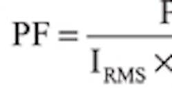
Harmonics minimization requires an understanding of power factor (PF), defined as:
Where:
P = Real power in watts
IRMS = RMS line current
VRMS = RMS line voltage
VRMS × IRMS = Apparent power in volt-amperes (VA)
Power Factor also equals the cosine of the phase angle () between line current and voltage; re-writing Equation (1):
The value of is a decimal number between 0 and 1.
The LT3798 uses one of the techniques that provide active power factor correction (PFC). There are techniques for passive power factor correction using resistors and capacitors, but they are not as effective as active PFC, so they produce higher harmonic levels.
Related Articles
True Bridgeless PFC Converter Achieves Over 98% Efficiency, 0.999 Power Factor
Flyback Design for Continuous Mode of Operation
About the Author

Sam Davis
Sam Davis was the editor-in-chief of Power Electronics Technology magazine and website that is now part of Electronic Design. He has 18 years experience in electronic engineering design and management, six years in public relations and 25 years as a trade press editor. He holds a BSEE from Case-Western Reserve University, and did graduate work at the same school and UCLA. Sam was the editor for PCIM, the predecessor to Power Electronics Technology, from 1984 to 2004. His engineering experience includes circuit and system design for Litton Systems, Bunker-Ramo, Rocketdyne, and Clevite Corporation.. Design tasks included analog circuits, display systems, power supplies, underwater ordnance systems, and test systems. He also served as a program manager for a Litton Systems Navy program.
Sam is the author of Computer Data Displays, a book published by Prentice-Hall in the U.S. and Japan in 1969. He is also a recipient of the Jesse Neal Award for trade press editorial excellence, and has one patent for naval ship construction that simplifies electronic system integration.
You can also check out his Power Electronics blog.
Comment About the Article
To join the conversation, and become an exclusive member of Electronic Design, create an account today!

Leaders relevant to this article: