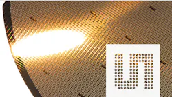
After the introduction of their 3D IC integration technology that enables the design and production of IC packages that are smaller, cheaper, and less vulnerable to electro-magnetic interference (EMI), ams is investing over $39 million in dedicated production equipment. The equipment will be installed in a clean room space at ams’ wafer fabrication plant near Graz, Austria and will be fully operational by the end of 2013. The increase in production capacity comes in response to a surge in demand outlook and will initially be directed towards the production of devices in the medical imaging and mobile phone markets.
Applications of the technology include the production of through-silicon via (TSV) interconnects that can replace bond wires in conventional single-die devices. It also enables the assembly of stacked-die devices where two die produced in different processes are bonded back-to-back. These stacked-die devices can replace two separate packages, have a smaller footprint and shorter interconnects, and can reduce electrical noise.
About the Author
Iliza Sokol
Associate Content Producer
Iliza joined the Penton Media group in 2013 after graduating from the Fashion Institute of Technology with a BS in Advertising and Marketing Communications. Prior to joining the staff, she worked at NYLON Magazine and a ghostwriting firm based in New York.
