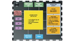
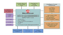
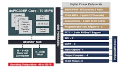
The dsPIC30F1010/202X 16-bit digital signal controllers (DSCs) from Microchip Technology were hailed as a new generation of digitally controlled power conversion ICs in 2006 when they were introduced (Fig. 1). The second generation of 16-bit DSCs in 2010 (Fig. 2) added more enhancements. Now, the 16-bit 2015 version, shown in Fig. 3, adds even more improvements for digital power-conversion system designs.
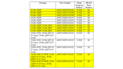
Compared to the two previous generations of DSCs, the 2015 14-member dsPIC33EP “GS” family from Microchip Technology is a major upgrade. This family provides the performance needed to implement more sophisticated non-linear, predictive, and adaptive control algorithms at higher switching frequencies. Advanced algorithms enable power-supply designs that are more energy-efficient and have better performance. Higher switching frequencies enable the development of physically smaller power supplies that offer higher densities and lower costs. Compared with the previous generation of digital-power DSCs, the new dsPIC33EP “GS” devices provide less than half the latency, when used in a three-pole three-zero compensator, and consume up to 80% less power in most applications. Table 1 lists characteristics of the 14 new “GS” DSCs.
Related
Key features of this new family include up to five 12-bit ADCs with as many as 22 ADC inputs, providing total throughput of 16 Msps with 300 ns ADC latency. For higher-precision designs, the dsPIC33EP “GS” devices include 12-bit DACs for each of four analog comparators. You can use two on-chip programmable gain amplifiers for current sensing and other precision measurements. Including these advanced analog amplifiers on the device reduces the number of external components required, thereby saving cost and board space. These features, combined with the overall high performance of the dsPIC33EP “GS” family, make it well suited for a wide range of applications, including : computer and telecom (ac/dc and dc/dc power supplies); industrial (solar inverters, LED lighting, HID lighting, battery chargers, projectors, and welders); and automotive (LED and HID headlights, dc/dc converters); among others.
This new dsPIC33EP “GS” family also includes advanced features, such as the Live Update Flash capability, which is especially helpful for high-availability or “always-on” systems. You can use Live Update to change the firmware of an operating power supply, including the active compensator calculation code, while maintaining continuous regulation. Variants from this new digital-power-optimized DSC family are available in an industry-smallest, 4 x 4 mm µQFN package for space-constrained designs.
Digital signal control opens the door to extensive creativity, limited only by the available features, the designer’s imagination, and the amount of available program and data memory. An example of a novel feature is the ability of a DSC to monitor the performance of an individual component within a power supply.
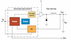
The best way to understand the functions of these DSCs is to check the simplified power supply version in Fig. 4. It shows the basic internal digital control configuration for a switch-mode power supply. These devices are configured within the supply’s feedback loop, so speed is critical because the A/D converter (ADC) and processor must sample the output and react as fast as possible to any changes. In operation, the ADC samples the power supply’s output voltage and sends the digital result to the processor that controls a pulse width modulator (PWM). Then, an external power stage rectifies the PWM output and produces a filtered dc output.
Compared with analog supplies, DSC ICs can provide extensive fault monitoring, better transient response, and lower-cost redundancy options. In addition, the digital approach eliminates power supply drift and the need for temperature compensation. This digital technique can program operational settings, which eliminates the manual tweaking of power-supply adjustments. DSC ICs perform these tasks primarily using firmware and in some cases sensors.
Digital signal control requires fewer hardware platforms because firmware can control power-supply performance while using identical internal hardware. Plus, this type of internal digital control can change topologies and configurations on-the-fly: from buck to boost or boost to buck, as well as from continuous to discontinuous. About the only necessary change might be to use different external power output stages. A unique aspect of these DSCs is that their analog comparators can terminate the pulse-width modulation (PWM) signal early, which allows cycle-by-cycle current limiting—a requirement for current-mode power supplies.
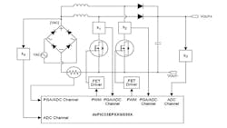
In addition, digital signal control enables the implementation of power factor correction (PFC) by adding appropriate firmware and some external hardware. Figure 5 is an interleaved PFC using a disPIC33EP DSC. An analog-based supply would require considerably more hardware. Furthermore, the same basic circuit could be used for uninterruptible power sources (UPSs), power inverters, and digital lighting. This degree of flexibility isn't available with an analog-based supply.
To be economically feasible, the DSC IC must cost-effectively provide the necessary high-speed power-supply functions. Besides the IC’s price, there are other cost-related issues, such as learning the digital-control design philosophy and developing the necessary firmware. But once this learning curve is mastered, a similar design approach can be used for all supplies.
Designers should ask themselves two necessary questions. First, what applications fit DSC-based power supplies? The obvious answer is ac-dc and dc-dc converters. The second question is, what power levels make the most economic sense? It all depends on the price-performance characteristics of the DSC IC.
Today, the cost of this controller IC could become a small percentage of the overall power-supply cost at 300 W and above. This could include front-end power supplies, high-power dc-dc converters, and bus converters. In the future, economies of scale could permit use of the DSC IC for power supplies below 100 W.
Digital 300 Watt ac/dc Power Supply with PFC
SMPS and digital power-conversion families include peripherals designed specifically for power-conversion applications such as 1 ns resolution PWM, 4 MSPS ADC, and on-chip high-speed analog comparators with integrated programmable reference voltages.
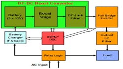
In this typical application the ac-dc design unit works with a universal input voltage range (85 - 165 VAC) and produces multiple dc outputs (Fig. 6). The design is based on a modular structure, which features three major power stages. The input stage is a PFC Boost Converter; the intermediate stage is a phase-shifted zero voltage transition (ZVT) converter, which includes a ZVT full-bridge converter and synchronous rectification; and the third stage is single- and multi-phase buck converters.
Implementing advanced software digital control loops for power applications requires a high-performance DSP engine along with specialized peripherals. The high-performance CPU and rich peripherals of the dsPIC DSC devices enable these solutions. These devices include peripherals specifically designed for power conversion. Peripherals such as a high-speed PWM, ADC, and analog comparators can be tied together using an internal configurable control fabric that enables them to interact directly with one another, resulting in performance gains in digital power conversion applications.
Digital Compensator Design Tool
Microchip’s new Digital Compensator Design Tool (DCDT) simplifies the process of analyzing the control-system performance and determining the digital compensator coefficients. The DCDT incorporates all feedback gains and delays to provide an accurate model of the control system. Along with analyzing the closed-loop performance via Bode Plots, the designer can verify stability by using the DCDT’s root locus and Nyquist plots. Once the desired performance is obtained, the DCDT will automatically calculate the compensator coefficients and scaling parameters and generate software files to be used with Microchip’s free SMPS Control Software Libraries.
Topology-independent, the DCDT allows analysis of the most sophisticated power converters. This architecture requires a mathematical expression of the plant-transfer function, which you can enter as a polynomial equation or in pole/zero form (up to 5th order systems). The tool also supports a data import option where the plant transfer function is a table of phase/gain versus frequency data points that can be generated from a simulation environment or even from a network analyzer.
The DCDT currently allows users to develop voltage mode and peak current mode control applications (average current mode control will be available soon). Depending on the control scheme, different compensators may be required. The DCDT supports the digital 3-pole/ 3-zero (3P3Z), digital 2P2Z, digital PID, and analog type II/III compensator types. The analog type II/III compensators allow analog designers to input their existing analog compensator designs into the tool either by passive R/C components or by entering pole/zero frequency points. The tool will then generate the equivalent digital compensator, streamlining the transition from analog to digital compensator design.
MPLAB Starter Kit for Digital Power
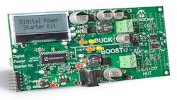
Documentation & Software The MPLAB Starter Kit for digital power uses the dsPIC33EP64GS502 DSC to implement a buck and a boost converter (Fig. 7). It is a digitally controlled power-supply board that consists of one independent DC/DC synchronous buck converter and one independent DC/DC boost converter. Each converter can drive its on-board MOSFET controlled resistive load or an external load. The board has an LCD display for voltage, current, temperature and fault conditions, and an integrated programmer/debugger, all powered by its 9 V power supply.
About the Author

Sam Davis
Sam Davis was the editor-in-chief of Power Electronics Technology magazine and website that is now part of Electronic Design. He has 18 years experience in electronic engineering design and management, six years in public relations and 25 years as a trade press editor. He holds a BSEE from Case-Western Reserve University, and did graduate work at the same school and UCLA. Sam was the editor for PCIM, the predecessor to Power Electronics Technology, from 1984 to 2004. His engineering experience includes circuit and system design for Litton Systems, Bunker-Ramo, Rocketdyne, and Clevite Corporation.. Design tasks included analog circuits, display systems, power supplies, underwater ordnance systems, and test systems. He also served as a program manager for a Litton Systems Navy program.
Sam is the author of Computer Data Displays, a book published by Prentice-Hall in the U.S. and Japan in 1969. He is also a recipient of the Jesse Neal Award for trade press editorial excellence, and has one patent for naval ship construction that simplifies electronic system integration.
You can also check out his Power Electronics blog.
Voice Your Opinion!
To join the conversation, and become an exclusive member of Electronic Design, create an account today!

Leaders relevant to this article:

