A prolific author of technical articles and books, Christophe P. Basso (ON Semiconductor, Toulouse, France) has written a new book, Linear Circuit Transfer Functions—An Introduction to Fast Analytical Techniques. This book consists of five chapters. The first chapter is a general introduction to the technique, explaining what transfer functions are and how time constants characterize a circuit. The second chapter digs into transfer function definitions and polynomial forms, introducing the low-Q approximation, and how to organize 2nd- and 3rd-order denominators or numerators. The third chapter uses the superposition theorem to gently introduce the extra-element theorem. Numerous examples are given to illustrate its usage in different 1st-order configurations. The fourth chapter deals with the 2-extra element theorem, generalized and applied to 2nd-order networks. Numerous examples illustrated with Mathcad and SPICE punctuate the explanations. Finally, the fifth chapter tackles 3rd- and 4th-order circuits, all illustrated with examples. Each chapter ends with 10 fully documented problems. There is no secret; mastering a technique requires patience and practice, and the author encourages the reader to test what he has learned after each chapter through these problems.
In Chapter 1, Basso reviews some of the founding theorems used extensively in the examples throughout his book. However, before tackling definitions and examples, he first described what the term transfer function means.
Assume you are in the laboratory testing a circuit encapsulated in a box featuring two connectors: one for the input, the second for the output. You do not know what is inside the box, despite the transparent case in the picture! You now inject a signal with a function generator to the input connector and observe the output waveform with an oscilloscope. Using the right terminology, you drive the circuit input and observe its response to the stimulus. The input waveform represents the excitation denoted u and it generates a response denoted y. In other words, the excitation variable propagates through the box, undergoes changes in phase, amplitude, perhaps induces distortion etc. and the oscilloscope reproduces the response on its screen.
The waveform displayed by the oscilloscope is a time-domain graph in which the horizontal axis x is graduated in seconds while the vertical axis y indicates the signal amplitude (positive or negative). Its dimension depends on the observed variable (volts, amperes and so on). The input waveform is denoted in lower case as it is an instantaneous signal, observed at a time - the instant t - u(t). A similar notation applies to the output signal, y(t). In Fig. 1.1, you see a low-duty ratio square-wave injected in the box engendering a rather distorted waveform on the output.
This ringing signal tells us that the box could associate resonant elements, probably capacitors and inductors but not much more than that. If we change the excitation, what type of shape will we obtain? Knowing what is inside the box will let us predict its response to various types of excitation signals.
There are several available ways to characterize an electrical linear circuit. One of them is called harmonic analysis. The input signal is replaced by a sinusoidal waveform and you observe how the stimulus propagates through the box to form the response. This is shown in Fig. 1.2.
The excitation level must be of reasonable amplitude—understand small—so that the response signal is not distorted. The input signal dc bias must also be set accounting for the physical constraints imposed by the active circuit so that upper- or lower-rail saturation is avoided. In other words, the box internal circuitry is not overdriven and remains linear during the analysis. Linearity is confirmed if the output signal is sinusoidal with the same frequency as the input sine and only varies in amplitude and phase while you ac-sweep the network. This is a so-called small-signal analysis. In the Laplace domain, you perform such harmonic analysis when you set s = jw in which w = 2.pi.f represents the angular frequency expressed in radians per seconds (rads/s). Laplace analysis with s = jw applies to linear circuits only.
Should you increase the input signal amplitude or change the operating bias point, slewing or clipping may happen. In this case, you explore the box large-signal or nonlinear response. This is a characterization different than the small-signal approach and it offers another insight into the circuit operation. Let us keep linear and once the right input amplitude is found, i.e., a signal of comfortable amplitude is observed on the oscilloscope screen, the frequency is varied step by step while output amplitude/phase couples are recorded in an array. At each frequency point f, we store the ratio of the response amplitude Y(f) in volts to the excitation amplitude U(f) in volts also. At each frequency point f, we save the phase information linking both input and output waveforms. As U and Y are complex variables affected by a magnitude and a phase, we can write:
AV represents a transfer function, a mathematical relationship linking a response signal Y to an excitation signal U. Please note that the excitation signal U resides in the transfer function denominator while the response Y sits in the numerator. It will always be this way throughout the book.
The transfer function is a complex variable characterized by a magnitude noted | Av (f)| and an argument, ÄAv (f) also noted arg Av(f) . The ratios Y(f)/U(f) we have stored correspond to the transfer function magnitude (also called modulus) observed at a frequency f while the phase difference between Y and U represents the transfer function argument or phase at the considered frequency. The transfer function magnitude dimension depends on the observed variables as we will later see. Here, because volts are involved for both variables, the transfer function magnitude is dimensionless or unitless. Furthermore, |AV| can only be greater than or equal to zero. It is what makes the difference between an amplitude which can take on any value, positive, null or negative and a magnitude which can only be zero or positive. If it is 0, there is no output signal. If |AV| is less than 1, we talk about attenuation. Now, if |AV| is greater than 1, it is designated as a gain. If the magnitude can only be a null or positive number, what about a gain of -2 then? It simply characterizes a stage offering a gain of 2, lagging or leading the excitation signal phase by 180°.
1.1.1 Input and Output Ports
It is convenient to represent our box as a two-port circuit. A port is a pair of connections that can input or output signals such as voltage and current. Figure 1.3 shows an illustration of this principle where you see two connecting ports, one input and one output.
Under some conditions, a port can take on the input and output roles at the same time. Imagine you want to measure the output impedance of the box. To realize this measurement, you classically implement Fig. 1.4 where a current across the output terminals is injected while the voltage across the same terminals is observed. This is what is called a single injection, i.e., one stimulus and one response. In this experiment, the box input port is shorted (see Appendix 1A). The excitation variable is the current Iout(s) injected into the port while the response is the voltage VOUT(s) collected across the port's terminals. The output impedance Z obtained from the ratio of the port voltage to the injected current is a transfer function. It has the dimension of an impedance expressed in ohms:
(from Christophe: I correct the S into s as it should be)
IOUT, the excitation signal lies in the denominator while the response, VOUT, stands in the numerator. We will come back on this important peculiarity.
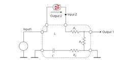
If input and output connectors are fixed, physical ports, which let you respectively inject and observe signals, nothing prevents one from creating other observation ports as needed. Simply remove a resistor, a capacitor or an inductor and its connecting points become a new port. This port can now be used as a new input stimulus or as an output variable you want to observe. As already mentioned, this newly created port can also play the role of an input and output port at the same time. In that case, the box originally featuring one input and one output, becomes a two-input/two-output system as illustrated in Fig. 1.5 in which the inductor has been removed. Using adequate terminology, we analyze the system by performing a double-injection: two stimuli—inputs 1 and 2—giving two responses, outputs 1 and 2.
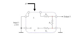
In this example, the voltage across the removed inductor terminals is the response while the injected current is the excitation signal. By dividing the port voltage by the injected current, we have the resistance offered by the port terminals when the element initially connected has been removed. In other words, we 'look' at the resistance offered by the inductor port as shown in Fig. 1.6 where the symbol R? and the arrow imply this exercise. Expressed in a different manner, we find the equivalent output resistance exhibited by the port when 'driving' the inductor, hence the name driving point resistance or driving point impedance abbreviated as DPI. Combining resistance and inductance gives us a time constant t ('tau') associated with this inductive element:
To conduct this exercise and find the resistance R, you can directly look at the sketch and infer the resistive series-parallel arrangement without solving a single equation. This exercise is called network inspection: you simply observe the network in certain conditions (for instance in dc, or when VIN is set to 0) and find resistance values by observing how components are connected together. For example, in Fig. 1.6, what resistance do you “see” looking into the inductor port while capacitor C is disconnected for the exercise? R1 appears first and then R3 in series goes to ground and returns to the inductor left terminal via the shorted input source. R2 is open and plays no role:
Applying (1.3) with (1.4) gives the definition for the time constant involving L:
A similar exercise can be conducted with the capacitor to also unveil the resistance R that drives this element. In this case, the time constant associated with the capacitance is simply:
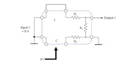
Assuming a shorted inductance in this particular illustration, what resistance value do you see in Fig. 1.7 when looking into the capacitor port? The left terminal is grounded while the second terminal also goes to ground via R2. R1 and R3play no role since their series combination goes from one ground to the other one. Therefore:
The time constant involving the capacitor is simply:
We have two storage elements, C and L, and there are two time constants. For each storage element, there is an associated time constant.
Rather than looking into a capacitive or an inductive port, we could also remove a resistor and define what resistance drives it, the exercise remains the same. Sometimes, looking into the port to 'see' the resistance is not as straightforward, especially when controlled sources are involved. In this case, you need to add a test current generator as in Fig. 1.5 and define the voltage generated across the considered terminals. The resistance offered by the port being the port voltage divided by the test current generator. This test generator will later be labeled IT and the voltage across its terminals VT.
What we just described is part of the technique foundations we will later explore: find resistances offered across the connecting terminals of resistive, capacitive or inductive elements once they have been temporarily removed from the circuit under certain conditions. Breaking a complex passive or active circuit into a succession of simple configurations where time constants are unveiled will help us characterize a network featuring poles and zeros. The Extra Element Theorem (EET) and later, the n Extra Element Theorem (nEET), make an extensive usage of these methods and it is important to understand this prerequisite. Appendix 1A will refresh our memory regarding available methods to derive output impedances.
1.4 Appendix1A—Finding Output Impedance/Resistance
As exemplified in the introductory figures, finding time constants associated with capacitors or inductors will often involve the derivation of the resistive term that ‘drives’ the considered capacitor or inductor. Besides capacitors and inductors, the exercise can also involve a simple resistor for which finding the resistance or impedance seen from its terminals is important. In other terms, what resistance is offered from the terminals the considered element is connected to?
There are several known methods to find the output impedance or resistance of a given network. They are reviewed in the appendix below. In the examples, we will use SPICE notations for the sake of simplicity: 1k = 103, 1Meg = 106, 1p = 10-12, 1n = 10- 9,1m = 10- 3and 1u = 10-6.
The Voltage Output Is Divided by Two
For the first option, assume you have a resistive divider made of two resistors driving a capacitor. You have removed the capacitor as in Fig. 1.7 and the circuit involving R1 and R2 appears in the left side of Figure 1.37. If you load that circuit with a resistance R, the output voltage takes a certain value VOUT, lower than VIN. The drop is incurred to the output resistance we want and the current delivered to the load. If you now load the same circuit with a resistance equal to the circuit output resistance RTH, as in the right side of Fig. 1.37, you obtain an output value exactly half of the voltage obtained with no load (IOUT= 0):
This voltage, VTH, is the Thévenin voltage and RTH the Thévenin output resistance we want.
Capitalizing on (1.63), you can write:
In this expression, the input voltage VIN does not play a role and disappears from both sides. If you solve (1.64) for RTH, you obtain the output resistance we want:
A Dynamic Output Resistance
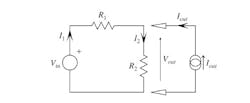
A second method of calculating the output voltage in relationship to a current injected by the generator IOUT, VOUT = f(IOUT). This is the method already introduced in Fig. 1.4. Assuming the same two-resistor circuit in Fig. 1.38, the output voltage across R2 can be defined as follows:
If you load the resistive network by a current source, the output voltage drops a certain quantity, proportional to IOUT and the network output resistance:
I1 is made of the output current IOUT and I2:
Substituting (1.67) into (1.66):
Rearranging and factoring VOUT on the left side leads to:
The incremental or small signal output resistance is found by differentiating (1.69) with respect to IOUT:
The word incremental refers to measurements involving small voltage (dV) and current (dI) variations around a defined operating point. We talk about small variations so that the system remains linear when measurements are performed. To that respect (1.70) is also referred to as the small-signal output resistance: the stimulus signal IOUT is purposely kept of small amplitude so that VOUT, the response remains undistorted.
Christophe Basso is a Technical Fellow at ON Semiconductor in Toulouse, France, where he leads an application team dedicated to developing new offline PWM controller’s specifications. He has originated numerous integrated circuits among which the NCP120X series has set new standards for low standby power converters.
Further to his 2008 book Switch-Mode Power Supplies: SPICE Simulations and Practical Designs, published by McGraw Hill, he released a new title in 2012 with Artech House, Designing Control Loops for Linear and Switching Power Supplies: a Tutorial Guide. He holds17 patents on power conversion and often publishes papers in conferences and trade magazines including How2Power and PET.
Christophe has over 20 years of power supply industry experience. Prior to joining ON Semiconductor in 1999, Christophe was an application engineer at Motorola Semiconductor in Toulouse. Before 1997, he worked at the European Synchrotron Radiation Facility in Grenoble, France, for 10 years. He holds a BSEE equivalent from the Montpellier University (France) and a MSEE from the Institut National Polytechnique of Toulouse (France). He is an IEEE Senior member.
Publisher
Linear Circuit Transfer Functions: An Introduction to Fast Analytical Techniques
By Christophe P. Basso
ISBN: 9781119236375
464 pages
May 2016, Wiley-IEEE Press
About the Author

Sam Davis
Sam Davis was the editor-in-chief of Power Electronics Technology magazine and website that is now part of Electronic Design. He has 18 years experience in electronic engineering design and management, six years in public relations and 25 years as a trade press editor. He holds a BSEE from Case-Western Reserve University, and did graduate work at the same school and UCLA. Sam was the editor for PCIM, the predecessor to Power Electronics Technology, from 1984 to 2004. His engineering experience includes circuit and system design for Litton Systems, Bunker-Ramo, Rocketdyne, and Clevite Corporation.. Design tasks included analog circuits, display systems, power supplies, underwater ordnance systems, and test systems. He also served as a program manager for a Litton Systems Navy program.
Sam is the author of Computer Data Displays, a book published by Prentice-Hall in the U.S. and Japan in 1969. He is also a recipient of the Jesse Neal Award for trade press editorial excellence, and has one patent for naval ship construction that simplifies electronic system integration.
You can also check out his Power Electronics blog.
Voice Your Opinion!
To join the conversation, and become an exclusive member of Electronic Design, create an account today!

Leaders relevant to this article:


