Understanding Test Challenges across the Power Semiconductor Life Cycle
The life cycle of a power semiconductor device involves a variety of test and characterization activities. Engineers face different measurement challenges in each stage throughout the process, from the early stages of designing a new power device to diagnosing faults and ultimately bringing the device to market.
In many cases, engineers find their education, training, and career paths direct them into very narrow areas of specialization. While they can develop expert-level knowledge in one or two areas, they can often have little understanding of the test and characterization challenges their colleagues may be facing in other areas of the product development lifecycle. This can be problematic when they need to step outside their comfort zone from time to time or need to work with other engineers but lack an appreciation of their challenges.
Let us look at what’s involved from a test and characterization perspective throughout the life cycle of a power semiconductor.
Evaluating Existing Devices
Applications engineers work with customers who are constantly stressing, testing, or stretching a design to maximize efficiency. These customers need detail beyond what is noted in the device specification. Requirements are constantly in flux, so what needs to be measured can vary daily. How can measurements be made quickly and easily without time being wasted to relearn software or instrumentation?
For these types of applications, it’s important to have a versatile set of test capabilities, including pulse, dc, and C-V. Software with a device-specific, as opposed to an instrument-specific, vocabulary helps simplify measurements. Such software can also simplify the interaction between multiple source measurement unit (SMU) instruments, so users can focus on the device rather than the instrumentation.
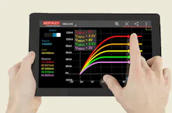
To make things even easier, vendors are starting offer smartphone and tablet apps (Fig. 1) that work with SMU Instruments to perform I-V characterization, including two- and three-terminal device testing and trend monitoring. These apps offer interactive analysis and insight into devices without programming. Applications include current versus voltage (I-V) testing on a variety of materials, two terminal and multi-terminal semiconductor devices, solar cells and embedded systems just to name a few.
Designing Devices
To effectively design devices that meet their customer’s latest requirements, power device design engineers and process engineers must understand how to tweak processes that produce the desired device performance. There must be confidence that the device models are sufficiently accurate, and changing particular process steps must produce the necessary changes in the device measurement parameters. Therefore, the device engineer must perform preliminary verification of key device parameters.
To help bring fully optimized devices to market in less time, parametric curve tracer instruments are now equipped with software that allows quick verification of key device parameters as well as complete device characterization including real-time trace mode (Fig. 2) for checking fundamental device parameters like breakdown voltage and full parametric mode for extracting precise device parameters. In addition to intuitive operation, these tools include large device libraries and built-in formulators to quickly relate measurement to device parameters.
Characterizing Performance
A characterization engineer provides the necessary measurement expertise and understanding of how measurement anomalies can affect non-targeted areas of device performance. It’s imperative to get results fast to enable multiple iterations with device or process engineers and quickly convert measurements to device parameters.
Measuring dc and capacitance parameters for high-power semiconductor devices requires sufficient expertise to optimize the accuracy of various measurements. Even for engineers with this level of expertise, managing setup changes between ON-state, OFF-state and capacitance-voltage (C-V) measurements can be time-consuming and prone to errors.
These challenges are especially difficult in the on-wafer environment. Characteristic curves for a power transistor, FET, or diode include a plot of its typical output characteristics. Output characteristics for some power devices can involve tens to hundreds of amps. Therefore, creating these curves requires a high-current instrument, such as an SMU (Source Measure Unit.) When multiple SMUs are configured in parallel, they can generate up to 100A in pulsed current, leading to challenges around managing resistance and inductance in cabling to insure accurate results.
To reduce the frustrations encountered when performing comprehensive dc I-V and C-V testing of power semiconductor devices, many engineers are adopting high-power interface panels (Fig. 3) that minimize connection changes between major measurement types. I-V and C-V measurements can be made through bias tees without connection changes and reduce opportunities for user error.
Preparing the Device for Production
To properly prepare a device for production, the production test engineers must prove if the device can be produced reliably. Measurements must be gathered for statistical setting of device specifications, and test times must be optimized to meet required production throughput. For these applications, multi-functional instruments offer the best way to obtain measurements quickly with minimal connection changes and switching.
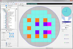
SMUs are multi-functional instruments that are proven for use in semiconductor applications. SMU instruments with the addition of test scripts improve throughput because of their tight synchronization, built-in processors for complex operations, and decision-making performed within the instrument, thus minimizing communication times. The SMU instruments can be used in parametric curve tracer configurations for interactive testing and for automated production testing. Automated software (Fig. 4) is available that combines advanced semiconductor test capabilities with control, data reporting, and statistics.
Meeting Reliability Standards
To conclude that a device meets reliability standards for commercial use, reliability test engineers have several responsibilities:
- Determining if a device will survive environmental stresses and continue to meet specifications
- Answering customer questions about device lifetime (MTBF, MTTF)
- Providing key insight into whether a device is fit for certain high-reliability applications including military/defense, aerospace, and automotive
Creating statistically relevant results requires sufficient sample sizes of the test devices. The nature of stress-measure cycling over many devices necessitates multi-channel parallel tests with automated data evaluation.
Integrated test systems are typically used for these types of applications and can be custom built to accommodate a range of application environments. Such systems are controlled using software that performs stress-measure loop cycling with integrated decision making. A wide range of power supply and SMU instrument solutions are available to permit simultaneous power and testing of any number of devices.
Implementing the Device
Once a device is validated, it’s ready for commercial use. Anyone who purchases devices must verify that the device is within tolerance for their application to ensure that the expected power-efficiency gains will be achieved in the end product. As the device matures and becomes available from multiple suppliers, power device consumers want to quickly inspect incoming devices to identify and eliminate counterfeit devices to avoid potential failures in the end product.
Here the test arsenal includes programmable power supplies to power basic circuit boards, power analyzers, and oscilloscopes equipped with power analysis modules and high-voltage, current, and differential probes. Power analyzers are used to assess overall end-product performance. Oscilloscopes enable analysis of switching loss, harmonics, and safe operating area.
Diagnosing Device Failures
Failure analysis engineers must determine whether a failure has been caused by end-product use or by a design flaw that was previously overlooked. Once this determination has been made, design and process engineering must be made aware of the cause of the failure, so that either process or design changes can be implemented to prevent future failures.
It’s important that basic device specifications, both static and dynamic, can be measured quickly. The end-use application is mimicked in an effort to reproduce the failure. Parametric curve tracers that feature trace mode are useful for this type of analysis. Software tools with built-in stress-measure tests make it possible to replicate the conditions that are causing the device performance degradation.
Wilson Lee is a senior manager of marketing at Tektronix. Prior to joining Tektronix, Wilson has had over 25 years of technical marketing, technical sales leadership roles–with manufacturers such as CTS Electronic Components, as well technical/value add distributors such as Richardson RFPD, and Premier Farnell. Wilson has heavily focused on design within the RF/Wireless, Industrial Power, and Industrial Automation market segments.


