Paralleled GaN Transistors Boost Converter Power Up to 100kW
Characteristics of enhancement-mode (e-mode) GaN, such as positive temperature coefficient of RDS(ON) and a temperature-independent threshold voltage, make them excellent candidates for paralleling. GaN Systems’ GS66516T is a GaN transistor that has these characteristics so it can operate efficiently and reliably in a parallel configuration; its features are listed below. After analyzing its parasitics, paralleled GS66516T transistors will be designed into the prototype of a half-bridge capable of 240A rated current.
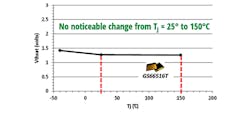
In parallel applications, the junction temperature of low RDS(ON) GaN transistors increase to balance current sharing during the ON state, because of positive temperature coefficiency of RDS(ON). On the other hand, the threshold voltage (Vth) of GaN Systems’ GS66516T is nearly constant as a function of junction temperature, as shown in Fig. 1. A device with lower Vth turns on earlier and turns off earlier, resulting in a higher turn-on switching loss and a lower turn-off switching loss. However, because of the characteristics of GaN, dynamic current sharing and switching loss distribution is not affected by unbalanced temperature distribution of paralleled transistors.
GaN Systems GS66516T features:
- 650 V enhancement mode GaN power switch
- Top-side cooled configuration
- RDS(ON) = 25 m
- IDS(max) = 60 A
- Ultra-low FOM (Figure of Merit = RDS(ON) × QG ) Island Technology® die
- Low-inductance GaNPX® package
- Gate drive requirements (0 V to 6 V)
- Transient tolerant gate drive (-20/+10 V )
- Switching frequency >10 MHz
- Fast and controllable fall and rise times
- Reverse current capability
- Zero reverse recovery loss
- 9 x 7.6 mm2 PCB footprint
- Dual gate and source sense pads for optimal board layout
- RoHS 6 compliant
Parasitics are the main challenge for configuring parallel operation of the power stage and gate driver circuits, which are sensitive to the high di/dt and dv/dt during the switching process. We need to remove bottlenecks of applying GaN to ~100 kW power electronics systems, which are not only limited to ZVS typologies but also hard switching applications.
Parasitic Inductance
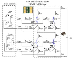
Figure 2 shows the equivalent circuit of a half- bridge power stage consisting of two high-side and two low-side GaN in parallel. This includes all the parasitic inductance in the gate drive loop and power commutation loop. It is necessary to understand the effects of parasitics and device characteristics on paralleled transistors when switching on.
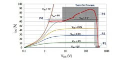
When the controller signal is added to the low-side gate driver, the higher switch of the totem pole circuit in the gate driver chip turns on. The gate driver capacitor begins to charge the CISS (CGS + CGD) of the paralleled GaN. When VGS>Vth (threshold voltage of GaN), the two-Dimensional Electron Gas (2DEG) begins conducting, as shown in Fig. 3. To simplify the analysis, we can divide the switching on process of paralleled GaNs into four periods: P1-delay period, P2-di/dt period, P3-dv/dt period, P4-remaining switching period.
Table 2 presents the effects and design rules of various parasitics in the gate drive loop and power loop. These parameters refer to the equivalent circuit in Fig. 2 of a half-bridge employing parallel GaN transistors.
Parasitic inductance is a function of the magnetic flux caused by the current. According to the law of electromagnetic induction, with the multi-layer magnetic-flux-canceling design strategy, the parasitics of the trace could be greatly reduced. The direction of the commutation current on two adjacent layers are opposite so that the generated flux outside the loop cancel each other.
Compared to Direct Bonded Copper (DBC) substrate, the PCB could easily adopt the multi-layer structure and smaller distance between layers to obtain a better magnetic flux canceling effect.
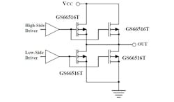
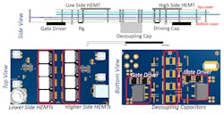
Figure 4 is the schematic of the half-bridge power stage consisting of four high-side and four low-side GaN transistors in parallel rated at 240A/650V. Figure 5 depicts the board layout of the half-bridge.
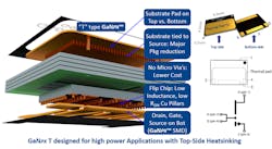
GaN Systems’ GaNPX packaging technology eliminates leads and bonding wires, which also aids circuit performance. Compared with using traditional TO-247 packages, this approach reduces stray inductance by >90% (Fig. 6).
The half bridge with four GaN transistors in parallel was modeled in Ansys Q3D. The power loop and gate-driver loop inductance were evaluated by Finite Element Analysis. The commutation loop inductance of the proposed design is only 0.7 nH, about one-fourth of the best available E-mode GaN-based power module. For each paralleled GaN transistor, quasi-common source inductance is <0.2 nH, and gate drive loop inductance is 4.2 nH.
Parasitic Capacitance
Parasitic capacitance is another design consideration. During the switch-on process, COSS as well as the reverse recovery charge (as seen in Si/SiC MOSFETs) increases the current spike and switching loss. Generally speaking, in hard switching application, the more transistors we parallel, the higher switching loss we get. There are an optimum number of paralleled GaN transistors to reach the highest efficiency for a specific application.
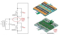
In Zero Voltage Switching (ZVS) application, during the dead time, the reactive energy stored on magnetic components begins to discharge and charge the parasitic capacitance. To secure ZVS, the reactive power has to be higher than the stored energy in the parasitic capacitance of GaN transistors and PCB board and the dead time loss of GaN transistors. On the other hand, to increase the efficiency of system, the reactive power needs to be controlled as close to the required energy as possible, which requires a precise modeling of parasitic capacitance. Parasitic capacitance of PCB and magnetic components can’t be ignored when compared with the ultra-small COSS of a GaN transistor. The PCB parasitic capacitance is modeled in Ansys Q3D in Figure 7.
The current spike measured during the hard switching-on in the lower switches is contributed by the displacement charge current of the parasitic capacitance between voltage jumping point and BUS+ node, which was measured in Fig. 8. The measured equivalent capacitance is about 2 nF.
Total parasitic capacitance of the half-bridge power stage is 3.2 nF (1.73 nF to BUS+ node, 1.48 nF to BUS- node).
Experimental Verification
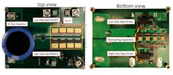
Figure 9 shows the prototype of a half-bridge power stage consisting of four high-side and four low-side GaN transistors in parallel that is rated at 240 A / 650 V. It has been experimentally verified by the double pulse test.
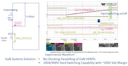
As shown in double pulse test waveform in Fig. 10, reliable hard switching on and off are realized at the rated power, 240 A/400 V with clean transition waveforms, while the spike on VDS during switching off is only 52 V even with close to 60 V/ns turn-off speed, which shows the benefit of low power loop inductance.
GaN parameters
- HEMT = High Electron Mobility Transistor
- RDS(ON) = On-state drain-to-source resistance
- CGS = Gate-to-source capacitance
- CGD = Gate-to-drain capacitance
- CISS = Input capacitance
- COSS = Output capacitance
- CRSS = Reverse transfer capacitance
- QG = Total gate charge
- VGS = Gate-to-source voltage
- VDS = Drain-to-source voltage
- IDS(max) = Maximum drain-source current
About the Author

Sam Davis Blog
Editor-In-Chief - Power Electronics
Sam Davis was the editor-in-chief of Power Electronics Technology magazine and website that is now part of Electronic Design. He has 18 years experience in electronic engineering design and management, six years in public relations and 25 years as a trade press editor. He holds a BSEE from Case-Western Reserve University, and did graduate work at the same school and UCLA. Sam was the editor for PCIM, the predecessor to Power Electronics Technology, from 1984 to 2004. His engineering experience includes circuit and system design for Litton Systems, Bunker-Ramo, Rocketdyne, and Clevite Corporation.. Design tasks included analog circuits, display systems, power supplies, underwater ordnance systems, and test systems. He also served as a program manager for a Litton Systems Navy program.
Sam is the author of Computer Data Displays, a book published by Prentice-Hall in the U.S. and Japan in 1969. He is also a recipient of the Jesse Neal Award for trade press editorial excellence, and has one patent for naval ship construction that simplifies electronic system integration.
Voice Your Opinion!
To join the conversation, and become an exclusive member of Electronic Design, create an account today!

Leaders relevant to this article:
