Supercapacitor-Based Backup Solutions: A Design Toolkit
Supercaps come in various shapes, sizes, and flavors, with vastly different specs. Some, for example, have ESRs of the order of tens of Ω but are very compact and low-cost and are suitable for low-energy applications whereas others with ESRs of 50 mΩ are suitable for providing bursts of high power for short durations. To make a solution reliable it must explicitly take into account these specs and the intended application so that maximum reliability and performance is obtained from a given product. Going a step further, it is also important to be able to conceptualize a solution that can take advantage of ongoing rapid improvements in supercap technology. Therefore, it is important to have a flexible platform for building complete and tailorable solutions around them.
The following “toolkit” of design ideas addresses a specific problem and suggests a solution — or the essence of it — in the form of a design “fragment”. This fragment in each case consists of a partial hardware schematic and a partial GreenPAK Designer diagram. A product designer can therefore pick the ones that are most relevant in a given context and integrate them into a custom solution. The GreenPAK Designer diagrams presented here are shown using the SLG46537V, Silego’s Configurable Mixed-signal IC (CMIC), but can be usually reconfigured to work on other GreenPAK products as well with only minor modifications, if at all.
Cell Mismatches
Cell mismatches can cause cell overvoltages. Supercapacitors rated for 5.5 V are often available as a stack of two cells with a rated voltage of 2.7 V each. Therefore, this requires cell balancing to ensure each cell stays within its rated voltage, as supercaps are susceptible to damage from overvoltage faults.
The simplest form of cell balancing is passive where each cell has a resistor across it and all resistors have the same value. Some energy is therefore continuously lost in the resistors. In fact, the value of these resistors decreases quite dramatically for higher-voltage applications. For example, with Murata’s 1F 5.5 V DMF4B5R5G105M3DTA0 supercaps[1], if the maximum voltage applied is 4.5 V, the balancing resistors are 47 kΩ, but if the maximum voltage is 5 V, the resistors must be 4.7 kΩ. A standard alternative usually proposed is active cell balancing. This, however, typically involves use of an op amp and a couple of MOSFETs. Figure 1 shows a different strategy using a Silego GreenPAK IC.
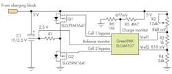
1. Cell balancing–schematic.
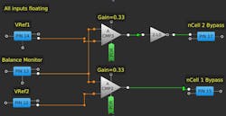
Figure 2 depicts the circuits inside of the SLG46537V. The SLG46537V monitors the overall charge state of the supercap. We need to use a voltage divider to monitor the supercap voltage for two reasons:
- Vdd of the SLG46537 may be lower than the fully-charged voltage of the supercap
- The ACMP2 and three op amps cannot take a reference voltage greater than 1.2 V.
2. Cell balancing – designer diagram.
Figure 1 shows the voltages present when the supercap is charged to 5 V. The voltages at the ends of R4, VRef1, and VRef2 are taken as the bounds for the cell-voltage difference. These voltages are taken as references for the two ACMPs depicted in the GreenPAK designer implementation (Figure 2) operated with a gain of 0.33 so that at a supercap voltage of 5 V, the balance terminal reflects as a voltage of 833 mV. If the balance terminal voltage is greater than VRef1, Q2 is turned on. When Q2 is turned on the midpoint voltage is dragged down, the upper cell’s charge current increases, and the lower cell is slightly discharged. When the balance terminal voltage goes below VRef2, Q1 is turned on. The value of R1 is decided by the speed of rebalancing desired but we can usually choose it to match the lowest value prescribed by the manufacturer for passive balancing (e.g., 4.7 kΩ for the Murata). During the rebalancing act, there is therefore some wasteful dissipation but this dissipation takes place only when an imbalance occurs, unlike with pure passive balancing when wasteful dissipation occurs all the time. Once the supercap is fully charged and balanced, both Q1 and Q2 are off and no wasteful dissipation occurs. This allows retention of charge for a significantly longer time.
When using Silego’s GreenFET (GFET) load switches instead of regular FETs, we must remember that the GFETs turn off when the input voltage is below 1.5 V. What that means is that as long as one cell is less than 1.5 V, it will not be bypassed even if the GFET across it gets a bias signal. Once both cells cross 1.5 V then the balancing is fully in effect. In practical terms what this means is that the cell voltages will not be equal at low voltages, which is usually not of any consequence.
In the lab test of this design fragment, we used two different 1.5 F supercaps of very different types instead of two cells of the same supercap. When charged without the balancing circuit, the voltage difference between the two was about 1.5 V when the stack was fully charged. When charged using the balancing circuit, the voltages advanced at different rates initially, till both reached 2.0 V. Thereafter, the voltages were matched to within 100mV till the stack was fully charged.
Maintaining a Fixed Output Voltage
A supercap's voltage, unlike that of a battery, decreases linearly as it is discharged. Therefore, we need a seamless transition from buck-to-boost conversion for a fixed output voltage to fully utilize the stored charge.
To hold the output voltage steady while the supercap voltage is either above or below the desired output voltage level, we need a buck-boost converter solution that handles the entire range of input voltage.
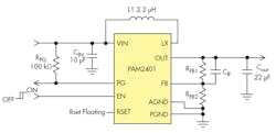
A simpler and lower-cost option is to have a Silego GPAK handle the buck conversion via PWM, but include a provision to switch over to an external boost converter IC when the supercap voltage falls below a set threshold. There are many choices of boost converters. One example is PAM2401 from Diodes Inc., which is able to provide an [adjustable] output of 3V3 from an input starting at 1V. Another candidate is Microchip’s MCP16251.
The typical application schematic for PAM2401 is shown in Figure 3. There is very little that is specific to this particular IC; most boost converters have very similar input/output wiring relationships, so for our purposes we can depict it as a black box with five connections, which may be added to a GPAK-based PWM control buck converter solution:
- Vin–Input
- PG–Power Good indicator (optional)
- EN–Chip enable
- Out–Output to load
- GND–Ground
3. A typical boost converter.
Detecting Aging or Electrolyte Dryup
A method is required to periodically test a supercap for aging or drying up before it fails. As described in Murata's Technical Note[1], the rise in ESR is a good indicator of impending aging or dryup failure. Therefore, the strategy consists in testing for the ESR at periodic intervals to gauge supercap health. (Note that the ESR at 1 kHz is usually smaller than that at dc.) When using a supercap in a ride-through application, where the power is being sourced for seconds to minutes, ESR must be measured at a low frequency. As described in [2], the ESR is best measured by charging the supercap to a given voltage, say 5 V, and then determining the instantaneous drop in output voltage when a load applied. What is important is that the load current for testing the ESR may be much greater than the application load per se. For example, if we take a high-quality 1F supercap that has an ESR of 50 mΩ and charge it to 5 V, we would need a load of 1 A to detect a drop of 50 mV.
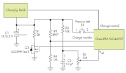
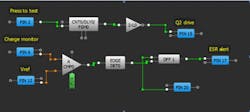
A candidate implementation of this strategy is shown in Figure 4 while the implementation in GreenPAK Designer is shown in Figure 5. It is assumed that the charging circuitry is under the control of the GPAK which will cut off charging when the supercap is fully charged. Figure 4 shows this as a digital output labeled “Charge control” that signals the charging block. It is best to test the ESR after the charge has been completed and the supercap voltage has stabilized.
4. ESR test – schematic
The momentary switch S1, “Press to test” feeds DLY2 which, operating as a one-shot using the 25kHz OSC0 clock, generates a pulse of approximately 120 µs. The pulse sends a low ON signal to Q2, which discharges the capacitor through a heavy load R1. During this discharge interval ACMP0 compares the supercap voltage against a reference that represents the voltage before the discharge started, and if the drop from a no-load state exceeds a predetermined value, an “ESR alert” is to be flagged to indicate that the ESR looks suspiciously high. EDGE DET0 and DFF1 latch the output so that the alert remains visible after the brief pulse test. DFF1’s data input is to be connected to Vdd but for lab testing it is connected to Pin 20.
5. ESR test – designer diagram.
The charger must be turned off for at least 15-20 seconds prior to conducting the test so that the voltage of the supercap has a chance to stabilize. How did we choose a discharge interval of 120 µs and what are reasonable values for this? Suppose we expect a nominal voltage drop of 50 mV due to ESR alone. The discharge duration must be small enough so that the drop in voltage at the end of the discharge period due to loss of charge per se is much less than 50 mV, say 1% of 50 mV or 0.5 mV. With a 1F capacitor being discharged at 1 A, this implies a maximum discharge duration of 0.5 ms. Further comparing this with the rise time of Q1, we see that the rise time of the SLG59M1641V FET is less than 5 us at 5 V. So choosing a pulse time of about 120 µs keeps the capacitor’s discharge minimal and is long enough compared to Q2’s rise time.
The reference voltage here is provided by the capacitor C2, which charges up through R2 to the same voltage as C1 during the charge cycle, but retains its voltage during the test discharge. For this to work reliably we have chosen the R2C2 time constant to be 0.1s, along with R3 >> R2.
Therefore, during the test discharge we can assert as follows for C2, assuming that the voltage across C1 has dropped by about 50 mV:
- Discharge current ~ 50 mV/10k = 5 µA
- Voltage drop rate = I/C = 5 µA/10µF = 500 mV/s
- Voltage at end of discharge period of 120 µs = 500 mV/s x .00012s = 0.06 mV
This shows that the voltage across C2 is practically constant during the test and therefore acts as a stable reference. R3’s setting determines the allowable voltage drop during the test. Note that we need the divider R3/R4 because the supercap may be charged up to 5 V which is greater than Vdd, and also because Vref needs to stay within the allowable range for the ACMP’s IN-pin (1.2 V).
Needless to say, the ESR test procedure must be conducted after making sure that primary power to the device being powered will not fail during the test, or that such failure will not be problematic!
When conducting a lab test of this design fragment, it is possible that a breadboarded environment may cause spurious results due to noise at the ACMP inputs. Adding a 1-10uF capacitor from R3’s wiper to ground can filter this noise. Further, when the SLG46537V Eval board is energized the DFF1 output may latch onto a High state. To get around this, the logic generator of the emulator is used to keep Pin 20 Low to start with, then the input is flipped to High before conducting the test. In tests this design reliably detected ESR “increases” of 500 mΩ, simulated by adding a small resistance of 500 mΩ in series with the supercap.
Monitoring Ambient Temperature
The life of a supercap can be affected significantly if operated at even mildly elevated temperatures. Supercaps are also relatively more sensitive to ripple current, which reflects in surface heating.
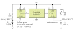
We are actually addressing two problems here. As described in [3], a 10°C; increase in ambient temperature causes the life of the capacitor to halve. In general it is good to operate the supercap at as low a temperature as practical. Further, supercaps are also sensitive to ripple current; there is an increase in surface temperature due to ripple current and we may measure this increase to determine if ripple is too high. The surface temperature rise in relation to ambient should not exceed 3°C. To accomplish these objectives we can have an analog temperature sensor physically attached to the supercap with another one mounted on the board to measure ambient temperature. Most low-cost analog temperature sensors have a sensitivity of 10 mV/°C – a good example is the MCP9700 from Microchip. The typical analog sensor consists of supply terminals and an analog voltage output. For the MCP9700 the output is specified at 500 mV at 25°C. Therefore, a surface temperature rise of 3°C leads to a differential output of 30 mV that needs to be detected.
In our scheme of things as illustrated in Figure 6, we have lifted the ground of the two sensors using two 1N914 diodes. The lift for the ambient temperature sensor is 530 mV, and that for the surface temperature sensor is 500 mV. We need diode D2 to be biased at about twice the current of D1 so that its drop is 30 mV higher. We bias the diodes at a current of about 100/200 uA respectively which is much higher than the supply current of the sensors themselves (6 uA) so that temperature variations of the sensor draw do not materially affect the ratio of the diode currents. The potentiometer may be used to set the difference to exactly 30 mV. Since it is the ratio of diode currents that sets the voltage drop difference, there is no effect of ambient temperature on this setting.
6. Temperature/ripple monitoring—schematic.
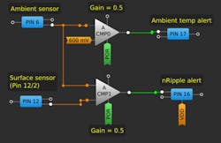
The part of the circuit that detects excessive ambient temperature is quite simple—the ambient sensor’s output is fed to the ACMP as shown in Figure 7 whose reference may be set appropriately. Since the sensor output is at 1 V at 25°C, we set a gain of 0.5 to stay with allowable limits for the ACMP. With a reference voltage of 600 mV, ACMP0 will trigger when the ambient temperature increases to 42°C. ACMP1, on the other hand, has as its reference half the voltage of the surface sensor, which is compared with the voltage of the ambient sensor (with a IN+ gain of 0.5). Therefore, ACMP1 changes state when the surface sensor output matches the ambient sensor output, at which point we can deduce that the surface temperature has exceeded ambient by 3°C and therefore that ripple current is too high.
In a given solution, the outputs of the ACMP can be used to trigger an alert, stop charging and so on. A more interesting action (not described here) would be to actually reduce the voltage at which the supercap is charged to if the temperature is too high, since it is the combination of temperature and voltage that causes degradation of life [3].
To test this design fragment, a supercap is of course not necessary — what we are primarily interested in is to test that the circuit can reliably test a temperature rise of 3°C or so. To do that the body of the surface sensor was touched with a finger while the ambient temperature was about 32°C. In a matter of seconds the nRippleAlert output started to flicker and then go low as the finger warmed up the sensor! Some initial calibration may be necessary due to the tolerances of the internal voltage dividers of the ACMP in 0.5x gain mode.
7. Temperature ripple monitoring—designer diagram.
Besides the problems discussed above, for completeness we include a few others that are relatively more straightforward to understand and address.
When a stack of supercapacitors is discharged rapidly and deeply, some cells may be subjected to negative voltage. To prevent this, we may add diodes across each cell that are normally reverse-biased, but become forward biased if the respective cell acquires a negative voltage.
Supercapacitors are sensitive to overvoltage. Overcharging can be addressed by using a Silego GreenPAK, such as the SLG46537V, to actively monitor the supercap voltage during the charge cycle and halting charge current as soon as the desired voltage is reached.
Supercaps hold a lot of energy and are capable of high current discharges when the ESR is as low as a few mΩ. It is important to have the usual methods for overcurrent protection which may be a fuse, circuit breaker or custom protection solution as shown with Silego ICs.
References
1. “Murata Supercapacitor Technical Note,” Document No. C2M1CXS-053K, Murata
Manufacturing Co. Ltd.
2. Section 16, “Supercapacitor Charging” in Analog Circuit Design Volume Three: Design Note Collection, Ed. Bob Dobkin and John Hamburger, Newnes, 2015.
3. “PowerStor Application Guidelines,” Cooper Bussmann Technical Note.
About the Author
Voice Your Opinion!
To join the conversation, and become an exclusive member of Electronic Design, create an account today!

Leaders relevant to this article:

