Download this article in PDF format.
The LTM8065 µModule regulator from Analog Devices’ Power Products Group (formerly Linear Technology) is a standalone non-isolated step-down switching dc-dc power supply that can deliver 3.5 A peak, or 2.5 A continuous. By implementing the low-EMI, Silent Switcher architecture, it complies with the CISPR22 Class B standard for domestic devices and apparatus. It comes in a thermally enhanced, compact, over-molded ball grid array (BGA) suitable for automated assembly by standard surface-mount equipment. Plus, it is RoHS-compliant.
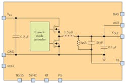
Integrated into the LTM8065 is a current-mode controller, power-switching elements, power inductor, and a modest amount of input and output capacitance (Fig. 1).
1. The LTM8065 µModule regulator’s internal components include a current-mode controller, power MOSFETs, resistor, capacitors, and inductor.
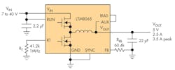
The specified input voltage range is 3.4 to 40 V, but you have to ensure the input voltage is high enough to support the desired output voltage and load current. In Figure 2 (see below), the input voltage is 7 to 40 V for a 5-V, 2.5-A continuous output.
You can pull the RUN pin below 0.9V to shut down the LTM8065, or tie it to 1.06 V or more for normal operation. When shut down, the LTM8065 only draws a few microamps.
An internal bias regulator powers its control circuits. Although this bias regulator normally draws power from the VIN pin, you can connect the BIAS pin to an external voltage higher than 3.2 V. Drawing bias power from an external source (such as a regulated voltage) improves the module’s efficiency.
Only a handful of external components are needed:
- CIN, 2.2- to 4.7-µF (0805) input capacitor (input bulk capacitor is required)
- COUT, 10- to 100-µF (0805 or 1206) output capacitor
- CFF, 10- to 47-pF feed-forward capacitor between AUX and FB (if needed)
- RFB, resistor to set the output from 0.97 V to 18 V
- RT, resistor to set the switching frequency from 200 kHz to 3 MHz
For most applications, the design process is straightforward:
1. Select the desired input range and output voltage.
2. Apply the CIN, COUT, RFB, and RT values.
3. Apply the CFF, as required.
4. Connect BIAS.
Capacitor Selection
If necessary, you can use larger values of CIN and COUT, which is generally acceptable and can yield improved dynamic response. Be sure to verify proper operation over the intended system’s line, load, and environmental conditions.
Use of ceramic capacitors aids the circuit because they are small, robust, and have very low ESR. For example, X5R and X7R types are stable over temperature and applied voltage and give dependable service. However, not all ceramic capacitors are suitable, such as the Y5V and Z5U. They have very large temperature and voltage coefficients of capacitance, so in an application circuit, they may exhibit a small fraction of their nominal capacitance, resulting in much higher output voltage ripple than expected.
Ceramic capacitors are also piezoelectric. In burst-mode operation, the LTM8065’s switching frequency depends on the load current, and can excite a ceramic capacitor at audio frequencies, generating audible noise. Because the LTM8065 operates at a lower current limit during burst-mode operation, noise is typically very quiet to a casual ear.
If this audible noise is unacceptable, use a high-performance electrolytic capacitor at the output. Also, you can employ a parallel combination of a ceramic capacitor and low-cost electrolytic capacitor.
Another precaution to using ceramic capacitors is the LTM8065’s maximum input voltage rating. A ceramic input capacitor combined with trace or cable inductance forms a high-Q (underdamped) tank circuit. Therefore, plugging the LTM8065 into a live supply could cause the input voltage to ring at twice its nominal value, possibly exceeding the device’s rating.
2. With 7 to 40 VIN, the LTM8065 step-down converter produces 5 VOUT.
You can select an optimal RT value to set the switching frequency; however, it may necessitate a different operating frequency. A frequency that is too high can reduce efficiency, generate excessive heat, or even damage the LTM8065 if the output is overloaded or short-circuited. A frequency that is too low can result in a final design with excessive output ripple or too large an output capacitor value.
Another choice is whether to implement soft-start. You can do this by connecting an external capacitor to the TR/SS pin. Alternatively, driving the TR/SS pin with a signal source or resistive network provides a tracking function. Do not drive the TR/SS pin with a low-impedance voltage source.
A Power Good output is available at the PG pin, which is the open-collector output of an internal comparator. PG remains low until the FB pin voltage is within about 10% of the final regulation voltage, and then goes high. The PG signal is valid when VIN is above 3.4 V. If VIN is above 3.4 V and RUN is low, PG will drive low.
Burst Mode
To enhance efficiency, the LTM8065 automatically switches to burst-mode operation in light or no-load situations. Between bursts, all circuitry associated with controlling the output switch is shut down, reducing the input supply current to just a few microamps.
You can also enable burst-mode operation tying SYNC to GND. To enhance efficiency at light loads, the LTM8065 automatically switches to burst-mode operation, which keeps the output capacitor charged to the proper voltage while minimizing the input quiescent current.
During burst-mode operation, the LTM8065 delivers single-cycle bursts of current to the output capacitor followed by sleep periods, in which most of the internal circuitry is powered off and energy is delivered to the load by the output capacitor. During the sleep time, VIN and BIAS quiescent currents are significantly reduced. Therefore, as the load current decreases toward a no-load condition, the percentage of time that the LTM8065 operates in sleep mode increases and the average input current is greatly reduced, resulting in higher light-load efficiency.
To select low-ripple burst-mode operation, tie the SYNC pin below about 0.4 V (this can be ground or a logic low output). To synchronize the LTM8065 oscillator to an external frequency, connect a square wave (with about 20% to 80% duty cycle) to the SYNC pin. The square-wave amplitude should have valleys that drop below 0.4 V and peaks above 1.5 V. The LTM8065 will not enter burst-mode operation at low output loads while synchronized to an external clock, but instead will pulse skip to maintain regulation.
You can synchronize the LTM8065 over its 200-kHz to 3-MHz range. For this, the RT resistor should be chosen to set the switching frequency equal to or below the lowest synchronization input. For example, if the synchronization signal will be 500 kHz or more, the RT should be selected for 500 kHz.
For some applications, it is desirable for the LTM8065 to operate in pulse-skipping mode, offering two major differences from burst-mode operation. The first is that the clock stays awake at all times and all switching cycles are aligned to the clock. The second is that full switching frequency is reached at lower output load than in burst-mode operation. These two differences come at the expense of increased quiescent current. To enable pulse-skipping mode, float the SYNC pin.
The LTM8065 features spread-spectrum operation to further reduce EMI/EMC emissions. To enable spread-spectrum operation, apply between 2.9 and 4.2V to the SYNC pin. In this mode, triangular frequency modulation is used to vary the switching frequency between the value programmed by RT to about 20% higher than that value. The modulation frequency is about 3 kHz.
For example, when the LTM8065 is programmed to 2 MHz, the frequency will vary from 2 to 2.4 MHz at a 3-kHz rate. When spread-spectrum operation is selected, it disables burst-mode operation, and the LTM8065 will run in pulse-skipping mode.
The LTM8065 employs frequency foldback that reduces the thermal and energy stress on the internal power elements during a short-circuit or output-overload condition. If the LTM8065 detects that the output has fallen out of regulation, the switching frequency reduces as a function of how far the output is below the target voltage. This limits the amount of energy that can be delivered to the load under fault.
During the startup time, frequency foldback is also active to limit the energy delivered to the potentially large output capacitance of the load. When a clock is applied to the SYNC pin, the SYNC pin is floated or held high, the frequency foldback is disabled, and the switching frequency will slow down only during overcurrent conditions.
Thermal Considerations
The maximum practical continuous load that the LTM8065 can drive actually depends on both the internal current limit and the internal temperature. The internal current limit is designed to prevent damage to the LTM8065 in the case of overload or short-circuit. The internal temperature of the LTM8065 depends on operating conditions, such as the ambient temperature, power delivered, and the system’s heat-sinking capability.
The LTM8065 output current may need to be derated if it is required to operate in a high ambient temperature. The amount of current derating depends on the input voltage, output power, and ambient temperature.
The die temperature of the LTM8065 must be lower than the maximum rating, so care should be taken in the circuit layout to ensure good heat sinking. The bulk of the heat flow out of the LTM8065 is through the bottom of the package and the pads into the printed circuit board (PCB). Consequently, a poor PCB can cause excessive heating, resulting in impaired performance or reliability.
Thermal shutdown inhibits power switching at high junction temperatures. The activation threshold of this function is above the maximum temperature rating to avoid interfering with normal operation. However, prolonged or repetitive operation under thermal shutdown may damage or impair the reliability of the device.


