Building a Power Supply Fit for Industrial Demands

The InnoSwitch3 highly-integrated switchers move the performance of flyback converters to a level that could only previously be achieved using complex two stage resonant converter topologies. InnoSwitch3 designs can reach efficiency levels of 94 %, reducing power supply losses by 25 % when compared to the best conventional high-efficiency flyback designs available today. This significant step in efficiency enables design engineers to produce small, highly-integrated, extremely efficient and cost-effective power supplies.
InnoSwitch3 ICs include a primary switching MOSFET with a dedicated controller, a secondary-side synchronous rectification driver, and a secondary-side controller, plus an integrated secondary to primary feedback mechanism (FluxLink) and a host of input and output protection features.
The new ICs employ a secondary side quasi-resonant (QR) controller which drives the synchronous rectification MOSFET and directs operation of the primary controller. The secondary controller uses a proprietary switching algorithm that provides constant high efficiency across the entire load range. QR (also known as valley-switching) forces the integrated primary-side MOSFET to turn on at the minimum switching voltage seen during the DCM ring. This significantly reduces switching losses and EMI.
InnoSwitch3 devices also incorporate FluxLink, Power Integrations’ magneto-inductive, isolated, high-speed communications link, between the primary and secondary sides. This provides a high-speed control interface between the low-voltage secondary side and high-voltage primary side controllers. Synchronous rectification enables higher efficiency, but requires accurate control of the timing of the secondary and primary switching MOSFETs to maximize efficiency while preventing switching overlap (which results in potentially-damaging cross conduction).
The FluxLink communication channel enables very precise control of both primary and secondary switches, maximizing efficiency while ensuring safe switching in both continuous and discontinuous conduction modes. Maximizing the on-time for the synchronous rectifier switch and eliminating diode conduction further improves efficiency. FluxLink also removes the need for an optocoupler, improving step-response, improving system reliability, and reducing component count. Figure 1 shows a typical applications circuit illustrating the high level of integration and low number of external components required.
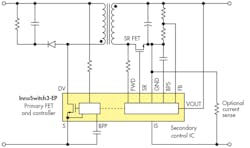
1. Typical application sequence.
InnoSwitch3 devices are UL1577, TUV (EN60950), and CQC China 5000m safety-approved. Their excellent EMI and noise immunity enables designs using them to achieve class A EN61000-4-8 (100 A/m) and EN61000-4-9 (1000 A/m) compliance. A new, lower-profile InSOP Halogen-free package has been introduced by Power Integrations for the InnoSwitch3 range that allows designs to easily meet the challenging CQC 5000 m China standard. This new package provides 6 kV reinforced isolation with over 11 mm creepage and clearance. All parts are 100% production-HPOT-tested to ensure quality and reliability.
The InnoSwitch3-EP (Embedded Power) IC family has been developed to address the unique requirements of industrial, scientific, and commercial applications, as well as supporting the needs of the appliance and lighting markets.
Industrial applications often have complex power requirements with multiple voltage rails to support the various functional elements like microcontrollers, sensors, analogue I/O, motors, networking, and wireless interfaces. Secondary-side control along with synchronous rectification improves the accuracy of voltage and current regulation for multiple output designs. Figure 2 demonstrates how a multi rail design can use weighted feedback to ensure the optimum control of the output rails compared to what can be achieved using a conventional Schottky diode-based design.

2. Multi-rail output using synchronous rectification and weighted feedback.
The advanced control algorithm and the speed of the integrated FluxLink communications link ensures extremely good transient response with almost undetectable undershoot or overshoot in response to a 100% load step. This is an important consideration in applications where some functions are turned on and off, such as motors and GSM wireless links. It is important that the output is well-controlled during these abrupt changes to ensure correct operation. Figure 3 illustrates the response of the InnoSwitch3-EP to a full load step change on the output rail.
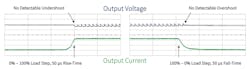
3. Transient response to a full-load step change.
The primary flyback circuit employs an integrated high voltage (725 V VDS(max)) MOSFET switch to deliver the high reliability typically expected by this market, and to support applications where equipment will be used in regions with unstable AC voltage supply. It also provides a high margin of safety in applications where the power supply is obliged to operate during line voltage swells. Companies designing for worldwide markets benefit from the additional reliability of the high voltage switch along with the protection offered by virtually lossless input line sensing.
Figure 4 shows the schematic for a universal input voltage (90V – 265V) dual output rail (5V and 12V) industrial power supply based on the INN3672C-H602 for fixed constant voltage/current control (CC/CV), output overvoltage is set at 120%, with an auto-restart response to a secondary fault condition along with hysteretic, auto-recovering over temperature protection.

4. RDR-611 universal input, dual-rail output, 10W open-frame power supply schematic.
This reference design shows the low component count and high efficiency is achievable with an InnoSwitch3-EP design. Fuse F1 provides protection in the event of component failure, while thermistor RT1 limits inrush current. The Pi filter consisting of C2, C3, and L1 provides differential noise filtering. An RCD clamp formed by C4, R8, R22, and D1 limits peak drain voltage spike caused by transformer leakage inductance.
One side of the transformer primary winding is directly connected to the rectified line voltage and the other side to the drain pin (D) of the internal 725V MOSFET. The circuit is self-starting using an internal current source to charge the primary ByPass pin (BPP) capacitor C6. During normal operation, an auxiliary winding is used to power the primary side via D7 and R6. Zener diode VR1 provides an additional (external) output overvoltage protection feature, using the bias winding voltage as a proxy for output voltage. Line over/undervoltage protection is provided by the V-pin fed via R3 and R4. In the event of a line overvoltage condition switching is disabled to protect the power stage.
The secondary side of the InnoSwitch3 is also self-powered from either the secondary winding forward voltage or the output voltage once it is established via the output voltage pin (VO).
Total output current is sensed via R12 situated between the current sense pin (IS) and ground. Output rectification is provided by Q1 for the 5V rail and Q2 for the 12V rail. L3 and L2 and capacitor C12 and C14 attenuate any high-frequency ripple and noise at the outputs. RC snubber networks have also been added across the synchronous switching FETS to dampen any high frequency ringing due to leakage inductance of the transformer windings reacting with the secondary trace capacitance. Resistors R16, R27, and R13 form a voltage divider network that is used to sense the output voltage from both outputs for improved cross regulation. Zener diode VR2 improves cross regulation when only the 5 V supply is heavily loaded.
Full details of reference design RDR-611—including full specification, schematics, printed circuit layout, bill of materials, performance data, and transformer design documentation—can be downloaded from the Power Integrations website.

About the Author
Andrew Smith
Product Marketing Manager
Comment About the Article
To join the conversation, and become an exclusive member of Electronic Design, create an account today!

Leaders relevant to this article: