Unique Test-and-Model Method Quickly Screens New Photovoltaic Materials
A novel approach to assessing newly developed photovoltaic (PV) materials could bypass today’s otherwise time-consuming steps in the process. At present, lab samples—usually composed of multiple layers of different materials bonded together—are needed for extensive testing.
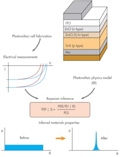
Now, however, a multidisciplinary team from MIT and other institutions has come up with a way to avoid much of the expensive and lengthy process of fabrication and testing. They used a series of relatively simple lab tests combined with computer modeling of the physical properties of the material itself, followed by additional modeling based on the Bayesian-inference statistical method.
1. By exposing the PV material to varying light intensities at different operating points, the team is able to quickly gather basic data that’s used for the analysis phase.
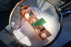
The new method requires making a simple test device and measuring its current output under different levels of illumination and different voltages (Fig. 1). This provides quantitative data on exactly how the performance varies under these changing conditions—this data is used to refine the statistical model (Fig. 2).
Tonio Buonassisi, an associate professor of mechanical engineering at MIT and senior author of the published paper, explained, “After we acquire many current-voltage measurements [of the sample] at different temperatures and illumination intensities, we need to figure out what combination of materials and interface variables make the best fit with our set of measurements.” He added, “Performing characterization takes time, sometimes weeks or months, and the measurements do not always have the necessary sensitivity to determine the root cause of any problems.”
Typical testing methods show the behavior of the “majority carriers,” but for PV materials, it’s actually the minority carriers—which are far less abundant—that limit a device’s overall efficiency, yet they’re much more difficult to measure. Typical procedures only measure the flow of current in the plane of a thin-film material, but it’s the up-down flow that’s actually used in a solar cell, and that flow can be drastically different.
2. The measured data is fed into the physical model, which is used to infer and then refine the material functional parameters and anticipated PV performance.
Buonassisi noted, “Representing each parameter as a probability distribution allows us to account for experimental uncertainty, and it also allows us to ‘suss out’ [discover] which parameters are covarying.”
Another consequence of the Bayesian inference process is that the estimates of each parameter can be updated based on new measurements, which continually refines the estimates and thus improves the precision of the result. As an added benefit, the new approach relies more on relatively inexpensive computing power and less on increasingly expensive lab equipment.
The multi-institutional team also included Riley Brandt '11, SM '13, PhD '16; former postdoc Vera Steinmann; MIT graduate students Daniil Kitchaev and Rachel Kurchin, and visiting professor Gerbrand Ceder; Chris Roat at Google Inc.; and Sergiu Levcenco and Thomas Unold at Hemholz Zentrum in Berlin. The work was supported by a Google Faculty Research Award, the U.S. Department of Energy, and a Total research grant through the MIT Energy Initiative.
In addition to the abstract, the full paper “Rapid Photovoltaic Device Characterization through Bayesian Parameter Estimation,” as published in the December 20th issue of Joule, is available online.
About the Author

Bill Schweber
Contributing Editor
Bill Schweber is an electronics engineer who has written three textbooks on electronic communications systems, as well as hundreds of technical articles, opinion columns, and product features. In past roles, he worked as a technical website manager for multiple topic-specific sites for EE Times, as well as both the Executive Editor and Analog Editor at EDN.
At Analog Devices Inc., Bill was in marketing communications (public relations). As a result, he has been on both sides of the technical PR function, presenting company products, stories, and messages to the media and also as the recipient of these.
Prior to the MarCom role at Analog, Bill was associate editor of their respected technical journal and worked in their product marketing and applications engineering groups. Before those roles, he was at Instron Corp., doing hands-on analog- and power-circuit design and systems integration for materials-testing machine controls.
Bill has an MSEE (Univ. of Mass) and BSEE (Columbia Univ.), is a Registered Professional Engineer, and holds an Advanced Class amateur radio license. He has also planned, written, and presented online courses on a variety of engineering topics, including MOSFET basics, ADC selection, and driving LEDs.
Voice Your Opinion!
To join the conversation, and become an exclusive member of Electronic Design, create an account today!

Leaders relevant to this article:


