72V Hybrid DC/DC Reduces Intermediate Bus Converter Size by up to 50%
Most intermediate bus converters (IBCs) provide isolation from input to output with the use of a bulky power transformer. They also normally require an inductor for output filtering. This type of converter is commonly used in datacom, telecom, and medical distributed power architectures. These IBCs are available from a wide variety of suppliers and are typically housed in an industry standard 1/16, 1/8, and ¼ brick footprints. A typical IBC has a nominal input voltage of 48V or 54V and produces a lower intermediate voltage between 5V to 12V with output power level from several hundred watts to several kilowatts. The intermediate bus voltage is used as the input to point-of-load regulators that will power FPGAs, microprocessors, ASICs, I/O, and other low-voltage downstream devices.
However, in many new applications, called “48V Direct,” isolation is not necessary in the IBC since the upstream 48V or 54V input is already isolated from the hazardous AC mains. In many applications, a hot-swap front-end device is required to use a non-isolated IBC. As a result, non-isolated IBCs are being designed into many new applications, which significantly reduce the solution size and cost while also increasing the operating efficiency and providing design flexibility. A typical distributed power architecture is shown in Fig. 1.
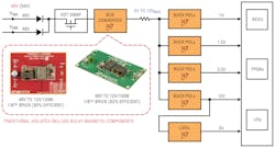
1. Typical Distributed Power Architecture
Now that non-isolated conversion is allowed in some distributed power architectures, one could consider using the single-stage buck converter for this application. It would need to operate over an input voltage range from 36V to 72V and produce a 5V to 12V output voltage. The LTC3891 from Analog Devices can be used for this approach and provides an efficiency of about 97% when operating at a relatively low 150kHz switching frequency. When operating the LTC3891 at higher frequencies results in a lower efficiency due to the MOSFET switching losses that occur with the relative high 48V input voltage.
A New Approach
An innovative approach combines a switched capacitor converter with a synchronous buck. The switched capacitor circuit reduces the input voltage by a factor of two and then feeds into the synchronous buck. This technique of reducing the input voltage in half and then bucking down to the desired output voltage results in a higher efficiency or a much smaller solution size by operating at a much higher switching frequency. Other benefits include lower switching losses and reduced MOSFET voltage stress due to the inherent soft-switching characteristic of the switched capacitor front-end converter resulting in lower EMI. Figure 2 shows how this combination has formed the Hybrid Step-Down Synchronous Controller.
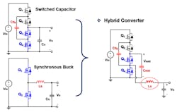
2. Switched Capacitor + Synchronous Buck = LTC7821 Hybrid Converter
New High-Efficiency Converter
The LTC7821 merges a switched capacitor circuit with a synchronous step-down converter, enabling up to a 50% reduction in DC/DC converter solution size compared to traditional buck-converter alternatives. This improvement is enabled by a 3X higher switching frequency without compromising efficiency. Alternatively, when operating at the same frequency, an LTC7821-based solution can provide up to a 3% higher efficiency. Other benefits include low EMI emissions due to a soft-switched front-end ideal for the next generation of non-isolated intermediate bus applications in power distribution, Datacom, and telecom as well as emerging 48V automotive systems.
The LTC7821 operates over a 10V to 72V (80V abs max) input voltage range and can produce output currents in multiple 10s of amps, depending on the choice of external components. External MOSFETs switch at a fixed frequency, programmable from 200kHz to 1.5MHz. In a typical 48V to 12V/20A application, an efficiency of 97% is attainable with the LTC7821 switching at 500kHz. The same efficiency can only be achieved in a traditional synchronous step-down converter by switching at one-third the operating frequency, forcing the use of much larger magnetics and output filter components. The LTC7821’s powerful 1Ω N-channel MOSFET gate drivers maximize efficiency and can drive multiple MOSFETs in parallel for higher-power applications. Due to its current mode-control architecture, multiple LTC7821s can be operated in a parallel, multiphase configuration with excellent current sharing and low output voltage ripple to enable much higher-power applications without hot spots.
The LTC7821 implements many protection features for robust performance in a wide range of applications. An LTC7821-based design also eliminates the inrush current typically associated with switched capacitor circuits by pre-balancing the capacitors on startup. The LTC7821 also monitors the system voltage, current and temperature for faults, and uses a sense resistor for overcurrent protection. It stops switching and pulls the /FAULT pin low when a fault condition occurs. An onboard timer can be set for appropriate restart/retry times. It’s EXTVCC pin permits the LTC7821 to be powered from the lower voltage output of the converter or other available sources up to 40V, reducing power dissipation and improving efficiency. Additional features include +/- 1% output voltage accuracy over temperature, a clock output for multiphase operation, a power good output signal, short-circuit protection, monotonic output voltage start-up, optional external reference, undervoltage lockout, and internal charge balance circuitry. Figure 3 shows the schematic of the LTC7821 when converting a 36V to 72V input to a 12V/20A output.
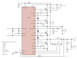
3. LTC7821 Schematic, 36VIN to 72VIn/12V/20A Output
The efficiency curves shown in Fig. 4 represent a comparison of three different converter types for the application that converts a 48VIN to a 12VOUT at 20A as follows:
- A single stage buck running at 125kHz with a 6V gate drive (Blue Curve)
- A single stage buck running at 200kHz with a 9V gate drive (Red Curve)
- The LTC7821 Hybrid running at 500kHz with a 6V gate drive (Green Curve)
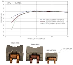
4. Efficiency Comparison & Transformer Size Reduction
An LTC7821-based circuit running at up to three times the operating frequency of the other converters has the same efficiency as the other solutions. This higher operating frequency results in a 56% reduction of the inductor size and up to a 50% reduction to the total solution size.
Capacitor Pre-Balancing
A switched capacitor converter usually has a very high inrush current when the input voltage is applied or when the converter is enabled, resulting in the possibility of supply damage. The LTC7821 has a proprietary scheme to pre-charge all switching capacitors before the converter PWM signal is enabled. Therefore, the inrush current during power-up is minimized. In addition, the LTC7821 also has a programmable fault protect window to further ensure reliable operation of the power converter. These features result in the output voltage having a smooth soft-start just like any other conventional current-mode buck converter. See the LTC7821 datasheet (http://cds.linear.com/docs/en/datasheet/7821f.pdf) for additional details.
Main Control Loop
Once the capacitor balancing phase is completed, normal operation begins. MOSFETs M1 and M3 are turned ON when the clock sets the RS latch, and turned off when the main current comparator, ICMP, resets the RS latch. MOSFETs M2 and M4 are then turned on. The peak inductor current at which ICMP resets the RS latch is controlled by the voltage on the ITH pin, which is the output of the error amplifier EA. The VFB pin receives the voltage feedback signal, which is compared to the internal reference voltage by the EA. When the load current increases, it causes a slight decrease in VFB relative to the 0.8V reference, which in turn causes the ITH voltage to increase until the average inductor current matches the new load current. After MOSFETs M1 and M3 have turned off, MOSFETs M2 and M4 are turned on until the beginning of the next cycle. During the switching of M1/M3 and M2/M4, capacitor CFLY is alternately connected in series with or parallel to CMID. The voltage at MID will be approximately at VIN/2. So, this converter just operates like a conventional current-mode buck converter with fast and accurate cycle-by-cycle current limit and option for current sharing.
Conclusion
The combination of a switched capacitor circuit to halve the input voltage followed by a synchronous step-down converter (hybrid converter) provides up to a 50% reduction in DC/DC converter solution size compared to traditional buck-converter alternatives. This improvement is enabled by a 3X higher switching frequency without compromising efficiency. Alternatively, the converter can operate with 3% higher efficiency in a footprint comparable to existing solutions. This new hybrid converter architecture also provides other benefits that include soft switching for reduced EMI and MOSFET stress. Multiple converters can be easily paralleled with active accurate current sharing when high power is needed.
About the Author
Bruce Haug
Product Marketing Manager, Analog Devices Inc.
Bruce Haug received his BSEE from San Jose State University in 1980. He joined Linear Technology (now a part of Analog Devices) as a product marketing engineer in April 2006. Bruce’s past experience includes stints at Cherokee International, Digital Power, and Ford Aerospace. He’s an avid sports participant.
Comment About the Article
To join the conversation, and become an exclusive member of Electronic Design, create an account today!

Leaders relevant to this article: