Defects in High-Voltage Ceramic Capacitors Found Acoustically
Within the body of a high-voltage multi-layer ceramic capacitor, a gap-type defect is beginning its career of destruction. The defect may be a void within the ceramic dielectric, a crack within the dielectric or a knit line delamination between the dielectric and the electrode. Any of these defects can grow until it creates a pathway between two electrodes. When current suddenly arcs from one electrode to the other, the capacitor will fail. It is likely to fail explosively and may in addition send a power surge that will damage the next component downstream. Smaller multi-layer ceramic chip capacitors have roughly similar defects, but those defects are more likely to slowly create numerous cracks in the surrounding dielectric until a typically non-explosive failure occurs.
The risk of electrical failure makes it sensible to inspect high-voltage ceramic capacitors before they are mounted on a board. Acoustic imaging tools such as the Sonoscan C-SAM tools are the weapon of choice here, in part because they are non-destructive, and in part because of the nature of the defects. The tool’s transducer launches a pulse of ultrasound at a given frequency into the top surface of the capacitor. The pulse travels into the capacitor at a speed around 5,000 m/s. There are very few features in the capacitor that can reflect a significant portion of the pulse, with one major exception: the interface between the solid material of the capacitor and the air in the void or other defect reflects very nearly 100% of the pulse to the transducer. None of the pulse crosses the void (an ultrasonic pulse doesn’t travel through air), but the transducer receives a very high amplitude echo.
Ceramic chip capacitors differ markedly in their structure from other components. Plastic-packaged ICs could have, for example, large volumes of mold compound that are not in contact with other features. If a void in an IC’s mold compound is not near the die surface, a wire, or a lead finger, it can often be ignored because it has little or no chance of causing an electrical failure. But a ceramic chip capacitor consists largely of electrode-dielectric layers. The whole component has few non-active regions. A void or crack or other gap-type defect almost anywhere can generate a failure.
Anyone who has imaged multilayer ICs knows that after a pulse has encountered many material interfaces, it becomes weaker, and signals sent back from deeper layers may be weak or difficult to detect. At each interface, part of the ultrasound is transmitted across the interface and part is reflected. The operator can increase the gain (volume) to view a bit more deeply, but the results are limited.
Ceramic chip capacitors may have dozens or even hundreds of layers of electrode and dielectric and still be capable of being imaged acoustically over their entire depth. What is different is the nature of the interfaces. The degree of reflection from an interface depends on the differences in material properties between the two materials at the interface; specifically, the density and acoustic velocity of the two materials. But the electrode and ceramic materials in a capacitor have densities and acoustic velocities that result in very small reflection of ultrasound. When a pulse strikes the first interface, there is a very small reflection, and very high transmission. This is why the pulse is able to travel all way to the bottom of the capacitor and return to the transducer with viable return echo signals.
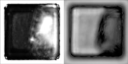
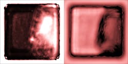
1. Reflection-mode C-SAM image (left) of a high-voltage capacitor having a large crack (white region and surrounding regions). At right, the same capacitor imaged by the Loss of Back Echo mode. Ultrasound returned from the bottom surface of the capacitor images the defect as a dark acoustic shadow.
Figure 1 is the C-SAM image of a high-voltage capacitor that has a large internal crack. The capacitor was imaged by two different imaging modes:
- At left is a bulk scan image, made using the reflection mode. In reflection-mode acoustic imaging, ultrasound is reflected from air-filled gaps like this crack. The very high amplitude of the return echoes over much of the crack tells software to image these regions in white. But it is hard to tell from this image what the real outline of the crack might be. There are mixed light and dark areas, which suggest that the crack may be undulating rather than flat. The capacitor itself is of course a reject, but a different imaging mode might tell more about the crack.
- Another imaging mode developed for the C-SAM tools is called Loss of Back Echo, or LBE. It depends on the fact that the transducer can be told to capture echoes from any time span between the insertion of the pulse into the sample and the arrival of echoes from the deepest part of the sample. The total flight time may be only a few millionths of a second, and within that time very short gates measured in nanoseconds can be set.
When LBE is used, the pulse is launched, but no echoes that are returned on its passage from the top of the capacitor to the bottom are recorded because no gate has been set within that time span. The gate is set at the bottom surface of the capacitor; from here the pulse—now an echo—begins its voyage back to the transducer. Any air-gap-related defect above the bottom surface will block the ultrasound from reaching the surface and no signal will be detected at the selected gate, creating a shadow at the back surface. In the case of the capacitor shown in Fig. 1, the crack will appear dark in the LBE image.
The results can be seen at right in Fig. 1. In the left part of the capacitor, the ultrasound has traveled to the bottom of the capacitor, been reflected, and returned with no change except some attenuation by the many interfaces it has passed through. The right area, however, is dark. Ultrasound pulsed into the top surface of the capacitor was reflected by the crack, but at a time relatively long before the echo from the bottom of the transducer arrived. In this area, no ultrasound was reflected by the bottom surface of the capacitor (it would have been reflected back toward the bottom if it had), and the area of the crack is dark and can be clearly discerned.
LBE is sometimes used to image other parts having relatively few internal features. More widely used, though (in addition to reflection imaging), is THRU-Scan, a mode in which the ultrasound is pulsed into the top surface (as in LBE) but collected by a separate sensor below the part. Cracks and other gap-type defects appear as black acoustic shadows in the image, but—as in LBE—there is no information about the depth of any feature.
Although LBE is often the mode of choice for high-voltage ceramic chip capacitors, there are a dozen or so additional modes for C-SAM tools. One mode scans the entire thickness of the sample, but divides the return echoes into a desired number of gates, which are equivalent to regions of depth. The results are what one might obtain by physically slicing the part horizontally into a number of slices and then imaging each slice individually. But the acoustic “slices” are non-destructive and can all be made during a single scan of the sample. If detailed information, including depth, is needed about internal features, this is the mode to use. The operator can request 10 gates, or 100 gates. Each gate will produce its own acoustic image with no increase in scan time.
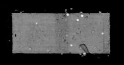
2. Small voids (white features) at the fifth of 8 gates set in a high-voltage capacitor. Darker features are shadows from defects in gates 1 through 4.
Figure 2 shows the acoustic image of a high-voltage capacitor different from the one shown in Fig. 1. The capacitor was “sliced” horizontally into 8 gates. Only those echoes from gate 5 were used for imaging Fig. 2.
The bright white features are small voids within gate 5. The darker features of about the same size are voids in gates 1 through 4, visible here because the pulse reflected from gate 5 encounters them and images them as acoustic shadows on its way back to the transducer. The large dark feature at lower right likewise lies above gate 5.
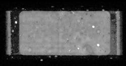
3. Gate 6: white features are in this gate; dark features are above it.
Figure 3 is the acoustic image of gate 6 in the same capacitor. The bright white features lie within gate 6. In the previous figure, a group of 3 white voids is visible just to the right of the top center of the gate 5 image. These voids are visible in gate 6 as dark acoustic shadows. Just to their right is a fourth dark feature—probably a void. It is not visible in gate 5, so it must lie in gate 4 or higher.
C-SAM® is a registered trademark of Sonoscan Inc.

About the Author
Tom Adams
Consultant, Nordson SONOSCAN
Tom Adams is a professional science writer based in New Jersey.
Comment About the Article
To join the conversation, and become an exclusive member of Electronic Design, create an account today!

Leaders relevant to this article: