µModule Boost Converter Squeezes into Space-Constrained Applications
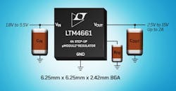
Analog Devices’ LTM4661 µModule synchronous boost converter leverages a miniaturized package size and minimum number of external components to fit into very small spaces. Its 6.25- × 6.25- × 2.42-mm ball-grid array (BGA) incorporates a dual-phase switching dc-dc controller, power MOSFETs, inductors, and supporting circuit components. Its only external requirements are three capacitors and one resistor that complete the design (Fig. 1). It operates from –40℃ to 125℃.
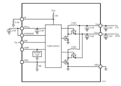
1. Simplified block diagram of the LTM4661 with a 3.3-V input and a 5-V at 2-A output.
Fig. 2 shows a LTM4661 demo board with its external components. The board reflects that the design strategy for the LTM4661 was to minimize the number of external components by incorporating several in the device, including:
- Switching frequency-setting resistor
- One of the two feedback resistors (sets VOUT)
- Internal frequency-compensation network
- Four power MOSFETs
- Two inductors (because the LTM4661 internal architecture is a dual-output, dual-phase synchronous boost regulator)
As seen in Fig. 1, it employs a dual-phase single-output architecture, rather than the conventional single phase of other boost converters. By interleaving two phases equally spaced 180° apart, both input and output current ripple get significantly reduced, as well as the amount of input and output decoupling capacitors required.
The LTM4661 operates from a 1.8- to 5.5-V input and will continue to operate down to a 0.7-V input after startup. You can set the output from 2.5 V to 15 V with a single external resistor. The combination of the small, thin package and wide input and output voltage range is ideal for many applications, such as optical modules, battery-powered equipment, battery-based backup systems, bias voltage for power amps or laser diodes, and small dc motors.
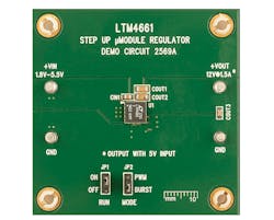
2. Shown is a demo board of the LTM4661.
The LTM4661 can deliver 4A continuously with 3.3 VIN to 5 VOUT, and 0.7 A continuously with 3.3 VIN to 12 VOUT. It delivers up to 92% conversion efficiency with 3.3 VIN to 5 VOUT.
Operating Frequency
Operating frequency is optimized to achieve the compact package size and minimum output ripple voltage while maintaining high efficiency. The default operating frequency is internally set to 1 MHz. In most applications, no additional frequency adjusting is needed.
If the application requires an operating frequency other than 1 MHz, it can be increased by adding a resistor, RFSET, between the FREQ pin and GND. The operating frequency can be calculated as:
fs = [(28 + RFSET)/RFSET]
where:
fS = switching frequency in MHz
RFSET = resistor between FREQ pin and GND in kW
You can synchronize to a desired frequency by applying a clock of twice the desired frequency to the SYNC/MODE pin. Also, the free-running frequency needs to be adjusted to a frequency approximately 80% of the desired frequency. For example, to synchronize to 1.5-MHz switching frequency, connect an external 3-MHz clock to the SYNC/MODE pin and add a 140-kΩ RFSET resistor between FREQ pin and GND to program the free-running frequency to 1.2 MHz.
The 1-MHz switching frequency and dual-phase single-output architecture enables fast transient response to line and load changes and significantly reduces output ripple voltage. There are three operation modes:
- Burst Mode operation
- Forced continuous mode
- External sync mode
The quiescent current in Burst Mode operation is only 25 µA, which provides extended battery run time. For applications demanding the lowest possible noise operation, the forced continuous mode or external sync mode minimize possible interference of switching noise.
Burst Mode operation is useful in applications where high efficiency at light load current are more important than output voltage ripple. To activate Burst Mode, connect the SYNC/MODE pin to GND. The output current (IOUT) capability in Burst Mode operation is significantly less than in continuous current mode (CCM) and varies with VIN and VOUT. The LTM4661 will operate in CCM mode even if Burst Mode operation is commanded during soft-start.
Only one phase of the LTM4661 is operational in Burst Mode operation; the other phase is disabled. The phase inductor current is initially charged to approximately 700 mA by turning on the N-channel MOSFET switch, at which point the N-channel switch is turned off and the P-channel synchronous switch is turned on, delivering current to the output. When the inductor current discharges to approximately zero, the cycle repeats.
In Burst Mode operation, energy is delivered to the output until the nominal regulation value is reached. Afterward, the LTM4661 transitions into a very low quiescent current sleep state. In sleep, the output switches are turned off and the LTM4661 consumes only 25 μA of quiescent current. When the output voltage droops approximately 1%, switching resumes. This maximizes efficiency at very light loads by minimizing switching and quiescent losses. Output voltage ripple in Burst Mode operation is typically 1% to 2% peak-to-peak. Additional output capacitance (22 μF or greater), or the addition of a small feedforward capacitor (10 to 50 pF) connected between VOUT and FB, can help further reduce the output ripple.
You can disable this boost converter by pulling SDB below 0.25 V and enable it by pulling SDB above 1.6 V. In addition, the SDB pin can be driven above VIN or VOUT, as long as it’s limited to less than its absolute maximum rating.
Starting Up
This µModule employs soft-start that utilizes a linearly increasing ramp reference voltage from zero to its nominal value of 1.2 V in approximately 10 ms, with the internal control loop driving VOUT from zero to its final programmed value. This limits the inrush current drawn from the input source. As a result, the duration of the soft-start is largely unaffected by the size of the output capacitor or the output regulation voltage. The soft-start period is reset by:
- Shutdown command on SDB
- UVLO event on INTVCC (INTVCC < 1.5V)
- Overvoltage event on VOUT (VOUT ≥ 16.5V)
- Overtemperature event (thermal shutdown, or TSD, is invoked when the die temperature exceeds 170°C). Upon removal of this fault condition, the LTM4661 will soft-start the output voltage.
Decoupling Capacitors
With current-mode control and internal feedback-loop compensation, the LTM4661 module has sufficient stability margins and good transient performance with a wide range of input and output capacitors.
For RMS ripple current decoupling, connect the µModule to a low ac impedance dc source and use one 10-μF input ceramic capacitor. You only need a bulk input capacitor when the input source impedance is compromised by long inductive leads, traces, or not enough source capacitance. The bulk capacitor can be an electrolytic aluminum or polymer capacitor.
To achieve low output voltage ripple and good transient response with a two-phase interleaving design, use a single 22-μF, low ESR output ceramic capacitor for the LTM4661. You can download the LTpowerCAD design tool for output ripple, stability, and transient-response analysis.
Output Disconnect
Output disconnect eliminates body-diode conduction of the internal P-channel MOSFET synchronous rectifiers. This allows VOUT to discharge to 0 V during shutdown and draws no current from the input source. Inrush current will also be limited at turn-on, minimizing surge currents seen by the input supply. Furthermore, the output disconnect feature allows VOUT to be pulled high, without backfeeding the power source connected to VIN.
This disconnect feature provides output short-circuit protection while maintaining a maximum set current limit. To reduce power dissipation under overload and short-circuit conditions, the peak switch current limits are reduced to approximately 2 A. Once VOUT exceeds approximately 1.5 V, the current limits are reset to their nominal values of 3.5-A peak switching current per phase.
An overvoltage condition can occur if VOUT exceeds approximately 16.5 V. This disables switching and resets the internal soft-start ramp. Once VOUT drops below approximately 16 V, a soft-start is initiated and switching is allowed to resume. If the boost converter output is lightly loaded such that the time constant of the output capacitance, COUT, and the output load resistance, ROUT, is near or greater than the soft-start time of approximately 10 ms, the soft-start ramp may end before or soon after switching resumes. This will defeat the inrush current limiting of the closed-loop soft-start following an overvoltage event.
If the die temperature exceeds 170°C, typical, the LTM4661 will go into TSD. All switches will be shut off until the die temperature drops by approximately 7°C, when the device reinitiates a soft-start and switching is re-enabled.
Layout Checklist
To optimize electrical and thermal performance, some layout considerations are necessary:
1. Use large PCB copper areas for high current paths, including VIN, GND, and VOUT. It helps to minimize the PCB conduction loss and thermal stress.
2. To minimize high-frequency noise, place high-frequency ceramic input and output capacitors next to the VIN, PGND, and VOUT pins.
3. Place a dedicated power ground layer underneath the unit.
4. To minimize the via conduction loss and reduce module thermal stress, use multiple vias for interconnection between the top layer and other power layers.
5. Do not put vias directly on the pad, unless they’re capped or plated over.
6. For parallel modules, tie the VOUT, VFB, and COMP pins together. Use an internal layer to closely connect these pins together.
7. Bring out test points on the signal pins for monitoring.

About the Author

Sam Davis
Sam Davis was the editor-in-chief of Power Electronics Technology magazine and website that is now part of Electronic Design. He has 18 years experience in electronic engineering design and management, six years in public relations and 25 years as a trade press editor. He holds a BSEE from Case-Western Reserve University, and did graduate work at the same school and UCLA. Sam was the editor for PCIM, the predecessor to Power Electronics Technology, from 1984 to 2004. His engineering experience includes circuit and system design for Litton Systems, Bunker-Ramo, Rocketdyne, and Clevite Corporation.. Design tasks included analog circuits, display systems, power supplies, underwater ordnance systems, and test systems. He also served as a program manager for a Litton Systems Navy program.
Sam is the author of Computer Data Displays, a book published by Prentice-Hall in the U.S. and Japan in 1969. He is also a recipient of the Jesse Neal Award for trade press editorial excellence, and has one patent for naval ship construction that simplifies electronic system integration.
You can also check out his Power Electronics blog.
Comment About the Article
To join the conversation, and become an exclusive member of Electronic Design, create an account today!

Leaders relevant to this article: