Switching regulators for space-constrained systems require attention to electronics, mechanical design, and system manufacturing considerations. The electronics details are usually viewed as the primary design considerations, but the other two factors are also important. For example, mechanical and manufacturing considerations play an important role in the VQFN-packaged LMR33630 from Texas Instruments. (The LMR33630 is also available in an 8-pin, 5 mm × 4 mm HSOIC.)
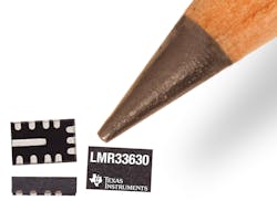
1. The point of a common pencil is almost the same size as the LMR33630’s 3 mm x 2 mm VQFN package.
The 12-pin VQFN demonstrates the impact of mechanical design by squeezing a 3A synchronous converter, including power MOSFETs, into a 3 mm × 2 mm HotROD VQFN package, as shown in Fig. 1.
System manufacturing considerations are also a factor because the LMR33630’s VQFN package has wettable flanks (Fig. 2), providing:
- Guaranteed visible side-wetting at good solder joints
- 100% visual inspection assembly processes
2. Wettable flanks improve the solder joints for the VQFN package.
In addition, this package features extremely small parasitic inductance and resistance, enabling very high efficiency while minimizing switch node ringing and dramatically reducing EMI. Its VIN/PGND pin layout is symmetrical on either side of the VQFN package, allowing the input current magnetic fields to partially cancel, which reduces EMI generation.
Electronic Characteristics
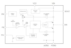
3. The LMR33630 is a synchronous buck regulator with a synchronous 3A output.
The LMR33630 is a synchronous peak-current-mode buck regulator IC (Fig. 3). It can accept a 3.3 V to 36 V input and provide a 1 V to 24 V output. The IC can drive a 3 A load with up to a 36 V input. And, it can produce a regulated 3.3 V output from a 3.8 V input. The regulator automatically switches modes between PFM and PWM, depending on the load. It features internal loop compensation, which reduces design time and requires fewer external components than externally compensated regulators.
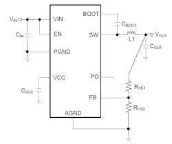
4. Simplified application with VOUT determined by RFBT and RFBB.
Figure 4 is a typical application circuit for the LMR33630. This device is designed to function over a wide range of external components and system parameters. Its internal compensation is optimized for a certain range of external inductance and output capacitance.
The EN voltage input controls start-up and shutdown. This input features precision thresholds, allowing the use of an external voltage divider to provide an adjustable input UVLO (undervoltage lockout). The value of EN voltage can:
- Cause the device to enter standby mode, powering the internal VCC, but not producing an output voltage.
- Enable the device, allowing it to begin a reference-based soft start that prevents output voltage overshoots and large inrush currents.
- Completely shut down the device.
The LMR33630 incorporates valley current limit for normal overloads and for short-circuit protection. In addition, the high-side power MOSFET is protected from excessive current by a peak current limit circuit. Cycle-by-cycle current limit is used for overloads, while hiccup mode is used for sustained short circuits. A zero current detector is used on the low-side power MOSFET to implement DEM at light loads.
Synchronous power converters can use the DEM (diode emulation mode) to improve efficiency. Many converters operates in CCM (continuous conduction mode), even though the load may be small. The current in the MOSFET switches can flow in either direction from source-to-drain which puts higher RMS currents on the switches and inductor. This leads to poor light-load efficiency. Diode emulation mode is used to achieve good efficiency at all loads.
Power-Good
A power-good output consists of an open drain NMOS, requiring an external pull up resistor to a suitable logic supply. It can also be pulled up to either VCC or VOUT, through a 100-kΩ resistor, as desired. Power-Good’s open-drain output goes low under fault conditions, such as current limit and thermal shutdown, as well as during normal start-up. A glitch filter prevents false flag operation for short excursions of the output voltage, such as during line and load transients. You can use the power-good flag function (PG) to reset a system microprocessor whenever the output voltage is out of regulation.
High-side-current limit trips when the peak inductor current reaches ISC, the switch current limit. This is a cycle-by-cycle current limit and does not produce any frequency or load current fold back. It is meant to protect the high-side MOSFET from excessive current. Under some conditions, such as high input voltages, this current limit may trip before the low-side protection. Under this condition, ISC determines the maximum output current (ISC varies with duty cycle).
Thermal shutdown protects the regulator from excessive junction temperature, TJ. When TJ reaches about 165°C the device shuts down; re-start occurs when the temperature falls to about 148°C.
Auto Mode
In auto mode the device moves between PWM and PFM as the load changes. At light loads the regulator operates in PFM. At higher loads the mode changes to PWM. The output current at which the device changes modes depends on the input voltage, inductor value, and nominal switching frequency.
In PWM mode the regulator operates as a constant frequency converter using PWM to regulate the output voltage. While operating in this mode the output voltage is regulated by switching at a constant frequency and modulating the duty cycle to control the power to the load. This provides excellent line and load regulation and low output voltage ripple.
Controlling Performance
The choice of switching frequency is a compromise between conversion efficiency and overall solution size. Lower switching frequency implies reduced switching losses and usually results in higher system efficiency. However, higher switching frequency allows use of smaller inductors and output capacitors, and hence a more compact design. Switching frequencies are fixed in three different VQFN versions: LMR33630ARNX, LMR33630BRNX, and LMR33630CRNX for 400kHx, 1.4MHz, and 2.1 MHz, respectively. For the HSOIC version replace “RNX” with “DDA.”
Setting the output voltage depends on the divider network consisting of RFBT and RFBB, which closes the loop between the output voltage and the converter. The converter regulates the output voltage by holding the voltage on the FB pin equal to the internal reference voltage, VREF.
Divider network resistance is a compromise between excessive noise pick-up and excessive loading of the output. Smaller values of resistance reduce noise sensitivity but also reduce the light-load efficiency. The recommended value for RFBT is 100 kΩ, with a maximum value of 1 MΩ. If a 1 MΩ is selected for RFBT, then a feed-forward capacitor must be used across this resistor to provide adequate loop phase margin.
Inductor selection depends on inductance value and saturation current. The inductance is based on the desired peak-to-peak ripple current and is normally chosen to be in the range of 20% to 40% of the maximum output current. The best value for inductor ripple current is 30% of the maximum load current.
Ideally, the saturation current rating of the inductor should be at least as large as the high-side switch current limit, ISC. This ensures that the inductor does not saturate even during a short circuit on the output. When the inductor core material saturates, the inductance falls to a very low value, causing the inductor current to rise very rapidly. Powered iron cores exhibit a soft saturation, allowing some relaxation in the current rating of the inductor. However, they have more core losses at frequencies typically above 1 MHz. Typically, the minimum inductor ripple current should be no less than about 10% of the device maximum rated current under nominal conditions.
The value of the output capacitor, and its ESR, determine the output voltage ripple and load transient performance. The output capacitor bank is usually limited by the load transient requirements, rather than the output voltage ripple. You can adjust the output capacitor and ESR to meet both the load transient and output ripple requirements. Ceramic capacitors can easily meet the minimum ESR requirements. In some cases an aluminum electrolytic capacitor can be placed in parallel with the ceramics to help build up the required value of capacitance.
The maximum value of total output capacitance should be limited to about 10 times the design value, or 1,000 μF (whichever is smaller). Large values of output capacitance can adversely affect the start-up behavior of the regulator as well as the loop stability.
Ceramic input capacitors provide a low impedance source for the regulator as well as supplying the ripple current and isolating switching noise from other circuits. A minimum of 10 μF of ceramic capacitance is required on the input of the LMR33630. This must be rated for at least the maximum input voltage that the application requires—preferably twice the maximum input voltage. This capacitance can be increased to help reduce input voltage ripple and/or maintain the input voltage during load transients. In addition, two small case size 220-nF ceramic capacitors should be used at the input, as close as possible to the VIN and GND pins on both sides of the regulator. The symmetrical placement of these small capacitors helps to improve bypassing of high-frequency currents and lower EMI.
The LMR33630 requires a boot-strap capacitor connected between the BOOT pin and the SW pin. This capacitor stores energy that is used to supply the gate drivers for the power MOSFETs. This requires a high-quality ceramic capacitor of 100 nF rated at least 10 V.
In some cases you can use a feed-forward capacitor (CFF) across RFBT to improve the load transient response or improve the loop-phase margin. This is especially true when values of RFBT > 100 kΩ are used. Large values of RFBT, in combination with the parasitic capacitance at the FB pin, can create a small signal pole that interferes with the loop stability. A CFF can help to mitigate this effect.
Temperature Considerations
When operating, the LMR33630 dissipates power that raises its internal temperature above ambient. Internal die temperature (TJ) is a function of the ambient temperature, the power loss, and the effective thermal resistance, RθJA of the device and PCB combination. The maximum internal die temperature for the LMR33630 must be limited to 125°C. This establishes a limit on the maximum device power dissipation and therefore the load current. Larger ambient temperatures (TA) and larger values of RθJA reduce the maximum available output current.
RθJA depends on many factors, such as power dissipation, air temperature/flow, PCB area, copper heat-sink area, the number of thermal vias under the package, and adjacent component placement. The HSOIC (DDA) package utilizes a die attach paddle, or thermal pad (PAD), to provide a place to solder down to the PCB heat-sinking copper. This provides a good heat conduction path from the regulator junction to the heat sink and must be properly soldered to the PCB heat sink copper. Due to the ultra-miniature size of the VQFN (RNX) package, a DAP is not available. This means that this package exhibits a somewhat larger value RθJA. However, as each pin of the VQFN package is very effective at thermal transfer because of the Flipped Die on leadframe (HotROD) construction. The Vin and Gnd pins should connect to large copper floods to spread heat from the device, allowing RθJA to be reduced from a Jedec layout significantly. In this way excellent thermal performance can be achieved in a very tiny package.
About the Author

Sam Davis
Sam Davis was the editor-in-chief of Power Electronics Technology magazine and website that is now part of Electronic Design. He has 18 years experience in electronic engineering design and management, six years in public relations and 25 years as a trade press editor. He holds a BSEE from Case-Western Reserve University, and did graduate work at the same school and UCLA. Sam was the editor for PCIM, the predecessor to Power Electronics Technology, from 1984 to 2004. His engineering experience includes circuit and system design for Litton Systems, Bunker-Ramo, Rocketdyne, and Clevite Corporation.. Design tasks included analog circuits, display systems, power supplies, underwater ordnance systems, and test systems. He also served as a program manager for a Litton Systems Navy program.
Sam is the author of Computer Data Displays, a book published by Prentice-Hall in the U.S. and Japan in 1969. He is also a recipient of the Jesse Neal Award for trade press editorial excellence, and has one patent for naval ship construction that simplifies electronic system integration.
You can also check out his Power Electronics blog.


