This Week in PowerBites: SiC Smorgasbord, EV Batteries’ Second Life, Even Faster e-Racers

This article is part of the This Week in PowerBites Library Series.
Injecting a Second Life into Used EV Batteries Becomes Easier with Distributed Storage Architecture

STABL Energy's unique electric power storage architecture makes it more practical and economical to give reclaimed EV batteries a second life in commercial-, industrial- and grid-scale storage systems. These systems, ranging in capacity from tens to many hundreds of kilowatt/hour (kWh) capacity, can be used to provide standalone power for remote buildings or EV charging stations, or support peak shaving and distributed load management as part of a smart grid.
Until now, large storage systems had to be built from collections of identical EV battery modules, hardwired to each other in a fixed configuration. STABL developed a dynamic interconnection system that makes it possible to employ a mix of modules of various voltages and capacities.
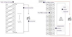
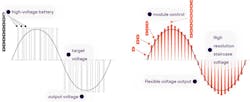
STABL is able to use a heterogeneous battery array thanks to a “modular multilevel inverter,” where the desired sinusoidal output voltage is produced by connecting individual battery modules in series to generate the desired voltage.
This technique is already widely used in high-voltage direct-current transmission, but the company optimized it for battery storage applications. As a result, the step voltage it generates is much closer to the desired grid voltage than that of ordinary battery storage inverters.
This distributed architecture allows STABL to connect discarded batteries with different residual capacities to the public power grid, even in larger quantities, without a central inverter. As an added benefit, the mains filter can be smaller, further reducing end-to-end losses.
To realize its architecture, STABL partnered with Infineon, which supplied the 100-V OptiMOS 5 low-loss, high-power MOSFETs required to implement the inverters. Dr. Arthur Singer, founder and co-CEO of STABL Energy, said that the company chose Infineon because of its products' low on-resistance, as well as high thermal performance and product reliability. "Compared to conventional systems, this reduces loss by up to 70% and cuts both operating costs and CO2 emissions by up to 40% per year," said Singer.
STABL's first storage units have passed CE and grid connection standards for Germany and have been connected to the country’s grid. An initial unit in Switzerland also has been connected—27 discarded KIA batteries with a nominal capacity of 98 kWh serve a residential neighborhood as temporary storage for solar energy.
Advanced SiC Gate Driver Helps Extend EV Range

The UCC5880-Q1 is a highly integrated, functional-safety-compliant, isolated gate driver optimized for silicon-carbide (SiC) MOSFETs that enables engineers to design more efficient traction inverters and maximize electric-vehicle (EV) driving range.
Developed by Texas Instruments, the driver offers features such as real-time variable gate-drive strength, an integrated SPI connection, advanced SiC monitoring and protection and functional safety diagnostics. These enable EV powertrain engineers to increase power density and reduce system design complexity while achieving their safety, cost, and performance goals.
The driver's most distinctive feature is the ability to vary the strength of its gate-driver signal in real-time, in steps between 20 and 5 A. This helps designers create SiC bridge inverters with lower switching power losses and can improve system efficiency by as much as 2%.
Depending on the vehicle, this improvement could add up to seven more miles of driving range per battery charge. For an EV user who charges their vehicle three times per week, the extra 2% efficiency could mean more than 1,000 additional miles per year.
In addition, the UCC5880-Q1’s SPI programmability and integrated monitoring and protection features can reduce design complexity as well as external component costs. Engineers can further reduce components and quickly prototype a more efficient traction-inverter system using the SiC EV Traction Inverter Reference Design. This customizable, tested design includes the UCC5880-Q1, a bias-supply power module, real-time control MCUs, and high-precision sensing.
For more information, read the technical article, “How to Maximize SiC Traction Inverter Efficiency with Real-Time Variable Gate Drive Strength.”
Package, Availability, and Pricing
Preproduction quantities of the automotive-grade, ISO26262-compliant UCC5880-Q1 are available now, only on TI.com, in a 10.5- × 7.5-mm, 32-pin shrink small-outline package (SSOP). Pricing starts at US$5.90 in 1,000-unit quantities. Designers can purchase a new UCC5880-Q1 evaluation module for US$249.
Half-Bridge Driver ICs with Active Miller Clamp Boost Ruggedness in High-Power Apps
Infineon Technologies added several new members to its EiceDRIVER 2ED132xS12x family of 1200-V silicon-on-isolator (SOI) three-phase gate drivers. SOI technology eliminates the parasitic thyristor structure and boosts robustness and immunity to negative transient voltages on the VS pin. The new devices offer increased output-current capabilities, extending the product line's range to higher system power levels.
The latest half-bridge drivers comprise four versions in two different packages: The 2ED132xS12M comes in a DSO-16 300-mil package and provides +2.3/−4.6-A current capability; the 2ED132xS12P comes in a DSO-20 300-mil package and supports +2.3/−2.3-A current drive capability. According to the company, the family features best-in-class switching performance in packages with sufficient creepage and clearance distances.
The drivers integrate a low-resistance (30 Ω) bootstrap diode, ultra-fast and accurate (±5% tolerance) overcurrent protection (OCP), enable input, fault-out, and programmable fault reset with separate logic (VSS) and output ground (COM) pins. The 2ED132xS12M variant provides additional features of the active Miller clamp (AMC) and short-circuit clamp (SCC).
Like all EiceDRIVER devices, they also offer robust negative VS transient immunity, shoot-through protection, undervoltage lockout, and fast overcurrent protection. These features help reduce the bill of materials and enable a more rugged design with a compact form factor suitable for high power applications such as commercial HVAC systems, heat pumps, servo drives, industrial inverters, pumps, and fans up to 10 kW. In addition, the devices are RoHS-compliant and resistant to electrostatic discharge (ESD) and moisture.
The EiceDRIVER 2ED132X series can be ordered now. In addition, the 2ED132x + 1200-V SiC EASY1B PIM evaluation board will be available in the coming months. More information is available at www.infineon.com/1200VHVIC.
SiC Modules, Bare-Die Devices Handle 10 kW to Multi-MW Apps in Rail, EV, Solar, Wind, and Storage

Navitas Semiconductor expanded its portfolio of SiC power modules and bare-die SiC devices, based on the company's GeneSiC trench-assisted planar-gate SiC MOSFET technology, to address higher-power applications. Target applications include centralized and string solar inverters, energy storage systems (ESS), industrial motion control, on-board and roadside EV chargers, wind energy, UPS, bidirectional microgrids, dc-dc converters, and solid-state circuit breakers.
With operating voltage ranging from 650 to 6,500 V, Navitas offers a lineup of discrete packages from 8-× 8-mm surface-mount QFNs to through-hole TO-247s. For customers who prefer to make their own high-power modules, all GeneSiC MOSFET and MPS diodes are available in bare-die format, with gold (Au) and aluminum (Al) top-side metallizations.
For applications requiring pre-integrated modules, the SiCPAK provides an initial, direct entry point into higher-power applications. SiCPAK modules employ “press-fit” technology to offer compact form factors for power circuits and deliver cost-effective, rugged, and reliable solutions to end users.
Within the lead-free SiCPAK, each SiC chip is silver (Ag) sintered to the module’s substrate for superior cooling and reliability. The substrate itself comprises “direct-bonded copper” (DBC) and is manufactured using an active-metal brazing (AMB) technique on silicon-nitride (Si3N4) ceramics, ideal for power-cycling applications. Examples include a SiCPAK half-bridge module, rated at 6 mW, at 1,200 V.
Multiple configurations of SiC MOSFETs and MPS diodes will be available to create application-specific modules for superior system performance. The initial release will include 1,200-V-rated half-bridge modules in 6-, 12-, 20-, and 30-mΩ ratings. A comprehensive power-module roadmap, with high-voltage SiC MOSFETs and MPS diodes, GaN power ICs, high-speed digital isolators, and low-voltage silicon control ICs is being mapped out. Parts are available now to qualified customers.
Iso-Buck IC Supports Protected Power Conversion and Gate Driving for IGBTs, WBG Transistors

The compact L6983i 10-W isolated buck (iso-buck) converter from STMicroelectronics offers high isolation, low quiescent current (2 µA), and a 3.5- to 38-V input-voltage range. Thanks to the iso-buck topology, the converter doesn’t require an optocoupler. It also integrates many important functions, resulting in more compact designs with significantly smaller BOM counts than conventional solutions.
The L6983i can be used to power isolated gate drivers for IGBTs and SiC or GaN transistors. It will also provide power for industrial automation, small traction systems and charging stations, and isolated safety equipment.
Capable of sourcing/sinking up to 4.5-A primary current, the L6983i offers many integrated functions such as adjustable soft-start time, internal loop compensation and power-good indicator, as well as protection from overcurrent and thermal shutdown. The converter's switching frequency can be adjusted from 200 kHz to 1 MHz and be externally synchronized. It also supports selectable spread-spectrum operation for improved EMC performance.
The evaluation board, STEVAL-L6983IV1, helps designers explore the features of the L6983i quickly and accelerate the time to market for new projects.
The L6983i, in production now, comes in a 3- × 3-mm QFN16 package, and is available from $1.38 for orders of 1,000 pieces.
e-Mode GAN FETs Increase Efficiencies, Cut BOM Counts in High- and Low-Voltage Apps

Nexperia complemented its line of cascode GaN power FETs with a new family of enhancement-mode (e-mode) devices, making it the only supplier to offer both cascode and e-mode GaN FETs. The seven new e-mode devices include five 650-V-rated e-mode GaN FETs, plus separate 150- and 100-V devices. Their high-level switching performance is attributable to very low Qg and QOSS values, while their low RDS(on) enables more power-efficient designs.
The five 650-V-rated devices feature extremely low RDS(on) values (between 80 and 190 mΩ). They come in a choice of 5- × 6-mm and 8- × 8-mm DFN packages. The FETs can be used to improve power-conversion efficiency in high-voltage, low-power (<650 V) datacom/telecom, consumer charging, solar and industrial applications, as well as boost the performance of brushless dc motors and micro server drives.
The new 100-V e-mode device has an RDS(on) of 3.2 mΩ and is housed in a WLCSP8 package. The 150-V, 7-mΩ device comes in a FCLGA package. Both of these devices are suitable for low-voltage (<150 V), high-power applications, such as high-efficiency dc-dc converters in data centers, fast-charging e-mobility and USB-C products, low-noise class D audio amplifiers, and more power-dense consumer devices like mobile phones, laptops, and games consoles.
Thanks to their high levels of integration and efficiency, these devices enable compact solution size in many power-conversion applications, and substantially reduce the bill of materials.
To learn more about the new e-mode GaN FETs, visit nexperia.com/gan-fets.
Ultra-Low-Profile Metal-Plate Shunt Resistors Eye Double-Sided Cooled Power Modules

According to ROHM Semiconductor, its PSR350 is the industry’s thinnest (0.03-in height) 12-W-rated metal-plate shunt resistor. It’s optimized for high-power applications in the automotive and industrial equipment markets. ROHM will also expand the PSR lineup to include a 0.2-mΩ (PSR100) model, along with a 15-W type in the industry’s smallest size (PSR330).
Conventional metal-plate shunt resistors reduce the cooling efficiency of power devices due to their relatively high profile. But decreasing height has proven difficult using existing materials and processes. ROHM has leveraged its strengths in manufacturing and design to develop the thinnest power shunt resistors on the market.
Optimizing material selection along with the manufacturing process achieves high rated power in a compact size. It also reduces the temperature coefficient of resistance compared to general products at the same rated power.
The PSR350, for example, utilizes the company’s vertically integrated production system, together with material and process optimization, to achieve a thickness of just 0.03 in. (0.85 mm), about half that of conventional products in the 12-W class. The same technology is used to develop the 0.25 × 0.25 in./ 64 × 64 mm PSR330. This decreases size by about 65% compared to conventional products in the same class, helping to reduce mounting area in a wide range of high-power applications.
At the same time, the PSR100 will be available in a 0.2-mΩ model that extends the lower limit from the existing 0.3 mΩ to enable detection of even higher currents.
For custom applications, ROHM’s vertically integrated production system allows for a quick development cycle through small-lot prototyping.
Application Examples
The new shunt resistors are suitable for high current sensing in applications equipped with motors and/or Li-ion batteries:
- Automotive: Electronic power steering (EPS), electric compressors, main inverters, onboard chargers, dc-dc, battery management system (BMS)
- Industrial equipment: Power modules, power tools, PV inverters, server power supplies, uninterruptible power supplies (UPS), base-station power supplies
- Consumer devices: Home appliances (e.g., air conditioners, refrigerators, vacuum cleaners, washing machines)
Formula E's 2023 Season Features 3rd-Gen Electric Racers with More Power, Smarts, and Speed

Now entering its 9th season of competition, the Formula E racing circuit will be thrilling e-geeks across the globe with the first appearance of a faster, more capable generation of vehicles that will battle for supremacy at speeds of over 200 mph. This year's schedule, which consists of 18 races held between January and July 2023 on street circuits in 13 of the world's leading cities, will test the cars' technologies in a wide range of grueling real-world environments.
The first generation of Formula E cars were the pinnacle of EV technology when they hit the track in 2014, They sport a 200-kW (230 kW peak) motor from McLaren Electronic systems and a 28-kWh Li-ion battery from Williams Advanced Engineering that could propel the car from 0 to 100 mph in three seconds and achieve top speeds of over 170 mph. Gen 3 not only greatly exceeds these parameters, but also introduces other advances in mechanical, electronic, and propulsion systems design that give them capabilities that rival their fossil-burning counterparts.

This year's Formula E vehicles pack much more power than their predecessors. They’re also the first-ever formula car to have front and rear powertrains. In addition to the 350-kW (470 hp) powertrain in the traditional rear location, Gen 3's front powertrain puts an additional 250 kW (335 hp) in the 760-kg (1,675.5 lb) chassis. With a total peak output in excess of 800 hp, the dual-motor drivetrain can propel the vehicle to over 322 kph / 200 mph.
Equally important, the cars' four-wheel traction systems allow them to hold higher speeds while navigating the twisty streets of cities like Monaco, Hyderabad, Berlin, and Portland. In addition, its four-wheel regenerative braking capabilities completely eliminate the need for conventional mechanical brakes, making it the first formula car to not have any hydraulic brakes on-board.
These and several other technical advances have helped make Formula E racing nearly as fast as the Formula 1 series it was spawned from. To learn more about the cars, and where you can see them in action, visit https://www.fiaformulae.com/en. And stay tuned for an upcoming feature that will take you on a deeper dive into the tech that powers Formula E.
Read more articles in the This Week in PowerBites Library Series.
About the Author

Lee Goldberg
Contributing Editor
Lee Goldberg is a self-identified “Recovering Engineer,” Maker/Hacker, Green-Tech Maven, Aviator, Gadfly, and Geek Dad. He spent the first 18 years of his career helping design microprocessors, embedded systems, renewable energy applications, and the occasional interplanetary spacecraft. After trading his ‘scope and soldering iron for a keyboard and a second career as a tech journalist, he’s spent the next two decades at several print and online engineering publications.
Lee’s current focus is power electronics, especially the technologies involved with energy efficiency, energy management, and renewable energy. This dovetails with his coverage of sustainable technologies and various environmental and social issues within the engineering community that he began in 1996. Lee also covers 3D printers, open-source hardware, and other Maker/Hacker technologies.
Lee holds a BSEE in Electrical Engineering from Thomas Edison College, and participated in a colloquium on technology, society, and the environment at Goddard College’s Institute for Social Ecology. His book, “Green Electronics/Green Bottom Line - A Commonsense Guide To Environmentally Responsible Engineering and Management,” was published by Newnes Press.
Lee, his wife Catherine, and his daughter Anwyn currently reside in the outskirts of Princeton N.J., where they masquerade as a typical suburban family.
Lee also writes the regular PowerBites series.
Comment About the Article
To join the conversation, and become an exclusive member of Electronic Design, create an account today!

Leaders relevant to this article: