This Week in PowerBites: Easier GaN Design, DoE Invites Students to Hack EVs

This article is part of the This Week in PowerBites Library Series.
What you’ll learn:
- How the DoE's EcoCAR EV Challenge is enabling engineering students to help guide the future of eco-car technology.
- Two new developments help facilitate the usage of GaN technology and expand the range of applications it can serve.
- New isolated gate drivers for SMPS.
Ohio State and Wilberforce University Team Win Phase One of DoE’s EcoCAR EV Challenge

The EcoCAR Electric Vehicle (EV) Challenge saw the Ohio State (OSU) and Wilberforce University team win Year One of the event, taking the lead in the four-year collegiate engineering competition. West Virginia University took second place and University of Alabama finished third in the judged competition, which was held from May 21-26, 2023 in Orlando, Florida.
The EcoCAR EV Challenge is a four-year collegiate engineering program that builds on the successful 35-year history of Department of Energy Advanced Vehicle Technology Competitions (AVTC) managed by Argonne National Laboratory and sponsored by the U.S. Department of Energy (DoE).* The cross-disciplinary competition among North American universities is designed to build an EV talent pipeline through cutting-edge automotive engineering education and practical application.

In this latest event, 15 participating teams are tasked with complex, real-world technical EV challenges. This includes enhancing the propulsion system of a 2023 Cadillac LYRIQ to optimize energy efficiency while maintaining consumer expectations for performance and driving experience throughout the four-year competition.
The OSU/Wilberforce team excelled across all judged categories in Year One, earning top three finishes for 12 of the pre-competition deliverables, 10n of which were first-place finishes. The Team will take home $10,000 in prize money from industry sponsors.
“Year One of EcoCAR is all about generating big ideas and developing a strategy for the remainder of the competition,” said Acting Assistant Secretary for Energy Efficiency and Renewable Energy Alejandro Moreno. “These students are already demonstrating the capacity and drive needed to pursue careers in the EV sector and become trailblazers in the mobility industry.”

In Year Two of the competition, each student team will receive a Cadillac LYRIQ, a next-generation battery electric vehicle (BEV) provided by GM. Teams will be tasked with reengineering the vehicle to add new energy-efficient and customer-friendly features designed to address the decarbonization needs of the automotive industry.
For more information about the EcoCAR EV Challenge, please visit avtcseries.org.
*Additional sponsors for this series include General Motors and MathWorks.
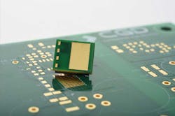
Space-Saving Octal High-Side Switches Feature Industrial-Focused Protection and Diagnostics

The IPS8160HQ and IPS8160HQ-1 high-side switches developed by STMicroelectronics provide eight channels in a compact QFN48L package, with the added value of built-in protection and diagnostics.
This unique combination of features helps designers save space and enhance reliability in PLC modules used for driving heavy loads and unidirectional motors in vending machines. Additional applications include I/O peripherals in factory automation equipment, computer-numerical-control (CNC) machines, and in general for controlling resistive, capacitive, and inductive loads with one side connected to ground. Both switches have low on-resistance (RDS(on)) of 160 mΩ (typ. at 25°C), which helps minimize power dissipation.
Overload (OVL) and junction overtemperature (OVT) protection for each channel prevent damage to circuits while minimizing any disruption caused by temporary faults. Overloaded channels turn off and restart automatically, keeping junction and case temperatures below safe maximum levels, while non-overloaded channels continue to operate normally. The device turns off immediately in the event of ground disconnection.
There’s also overvoltage protection, undervoltage lockout (UVLO), short-circuit protection, output-current limitation, and an overtemperature fault indicator.
The IPS8160HQ has a preset current limit of 0.7 A, while the IPS8160HQ-1’s current limit is 1 A. Both switches maintain an operating-voltage range from 10.5 to 36 V and facilitate meeting international standards for industrial equipment. These include IEC 61131-2 for process controllers and IEC 61000 specifications for electromagnetic compatibility (EMC), electrostatic-discharge (ESD) immunity, electrical fast-transient (EFT/burst) immunity, and surge immunity.
Users can quickly evaluate the IPS8160HQ and IPS8160HQ-1 driving and diagnostic capabilities with the X-NUCLEO-OUT9A1 and X-NUCLEO-OUT19A1 digital output expansion cards for STM32 Nucleo boards. They can be connected to 1-A industrial loads.
The IPS8160HQ and IPS8160HQ-1, in production now, come in an 8- × 6- × 0.9-mm-pitch QFN48L package. Pricing is $4.02 for orders of 1,000 pieces. For more information, visit www.st.com/ips8160hq.
Robust 650-V Merged-PiN SiC Diodes Boost Efficiency in Data Center, Industrial, Solar, TV Apps

Navitas Semiconductor released its fifth generation of high-speed GeneSiC silicon-carbide (SiC) power diodes, intended to meet the stringent requirements of data center, industrial motor-drive, solar, and consumer applications.
The 650 V-rated Merged-PiN Schottky (MPS) diodes integrate a unique PiN-Schottky structure. that exhibits “low-built-in voltage-biasing” (“low knee”) that gives the device enhanced robustness and very high operating efficiency across all load conditions. Applications include power factor correction (PFC) in server/telecom power supplies, industrial motor drives, solar inverters, LCD/LED TVs, and lighting.
The device's novel GeneSiC MPS structure combines the best features of both PiN and Schottky diode structures, producing the lowest forward-voltage (VF) drop of only 1.3 V, high surge-current capability (IFSM), and minimized temperature-independent switching losses. Proprietary thin-chip technology further reduces VF and improves thermal dissipation for cooler operation. These GeneSiC diodes are being offered in a low-profile, surface-mount QFN package for the first time.
To ensure reliable operation in critical applications, the 5th-gen, 650-V MPS diodes offer best-in-class robustness and ruggedness, including high surge-current and avalanche capability, with 100% avalanche (UIL) production testing.
Ranging from 4 to 24 A in an array of surface-mount (QFN, D2-PAK) and through-hole (TO-220, TO-247) packaging, the GExxMPS06x-series MPS diodes cover applications ranging from 300 to 3,000 W. Among some of the more diverse circuit possibilities are solar-panel boost converters and continuous-current-mode PFC in gaming consoles. With a “common-cathode” configuration, the TO-247-3 package offers great flexibility for high power density and bill-of-materials reduction in interleaved PFC topologies.
Improved Gate Structure Boosts Efficiency in N-Channel MOSFETs

In recent years, worldwide power consumption has been on the rise, driving the need for industrial equipment (e.g., servers and base stations, along with various motors) to become more efficient while still using cost-effective medium-voltage MOSFETs. However, these general-purpose MOSFETs are characterized by two main parameters leading to power losses: on-resistance (RDS(on)), which is inversely proportional to chip size, and gate-drain charge (Qgd) that increases proportionally with chip size, making it challenging to achieve both.
To improve the tradeoff between the two, ROHM Semiconductor adopted copper-clip connections and improved the gate structure in its RS6xxxxBx/RH6xxxxBx series of N-channel MOSFETs (40/60/80/100/150; 13 part numbers). They’re suitable for applications operating on 24/36/48-V power supplies, such as base stations, servers, and motors for industrial and consumer equipment.

The new MOSFETs are able to achieve an RDS(on) value of 2.1 mΩ—approximately 50% lower than conventional MOSFETs—by increasing device performance and adopting the HSOP8/HSMT8 package featuring low-resistance copper-clip connections. In addition, improving the element gate structure reduces Qgd, which is generally in a tradeoff relationship with RDS(on), by approximately 40% versus conventional products (comparing typical values for RDS(on) and Qgd for 60-V HSOP8 package products). These enhancements reduce both switching and conduction losses, greatly contributing to higher application efficiency.
Single-Chip AC Direct DC Power-Delivery Tech Approaches Commercialization

Amber Semiconductor recently announced that it has entered the manufacturing and integration phase for its patented AC Direct DC Enabler technology, a silicon solution that extracts dc directly from ac mains without the use of transformers, rectifier bridges, or filtering. The AC Direct DC Enabler silicon chip enables dynamic delivery of dc power on demand, and it requires only half the components of today’s standard, comparable systems.
With three output voltage rails (two fixed at 3.3 V and 5 V and the other is configurable from 1.8 to 24 V dc and up to 5 W of power), the AC Direct DC Enabler operates as a highly flexible primary power supply or housekeeping power for a wide range of products and technologies without the need for rectifier bridges, input filtering, or transformers.
The architecture enables a minimum two-thirds size reduction in footprint—or more, depending on the specific power requirements. Additional flexibility for system developers is afforded by the integrated SPI port, allowing for programmability of default values and accessibility to status bits within a control register file. Configuration of voltages, load current, and status monitoring of protection thresholds for current, voltage, and temperature operating parameters are determined by control bits within the register file, held in non-volatile memory.
Amber Semi’s silicon chip engineering samples will be available for customer demo testing later in 2023 into the start of 2024. The company is currently working with strategic customers to conduct ongoing evaluations of its AC Direct DC Enabler technology under non-disclosure agreements.
Upgraded Wireless Power System Now Delivers Up to 2 W with Increased Range

Energous Corp. launched a new 2-W conducted power transmitter that addresses the growing power demands from the rapidly expanding IoT ecosystem across supply chain, logistics, retail, industrial, and agricultural industries. The 2-W PowerBridge transmitter doubles the energizing capability of Energous’ 1-W transmitter currently deployed in the field, providing more range and making it possible to free many more IoT devices from batteries or charging cords.
Energous’ 2-W PowerBridge helps reduce the need for replaceable batteries and charging cables. It’s able to power IoT devices in these settings at distance and with less requirements for maintenance or human intervention, enabling a more automated workflow and deployment of Active Energy Wireless Power Networks.
These devices not only have the capability of wirelessly charging multiple devices simultaneously from a distance using RF-based wireless power, but they can also function as data links for connected IoT devices. As a result, they can communicate valuable data and insights back to the cloud.
The PowerBridge will be available for testing via the company’s 2-W Evaluation Kit by the end of Q2 2023.
Next-Gen Isolated Gate-Driver ICs Bring Higher Performance to SMPS Designs

Today’s 3.3-kW switched-mode power supplies (SMPS) can achieve power densities of 100 W/in.³ by utilizing the latest technologies. These include superjunction (SJ silicon) and silicon-carbide (SiC) power MOSFETs in the totem-pole PFC stage as well as gallium-nitride (GaN) power switches for high-voltage dc-dc stage operation.
To meet the latest design and application needs, Infineon Technologies introduced the next generation of its EiceDRIVER product family of dual-channel, galvanically isolated gate-driver ICs. The new portfolio combines robust isolation technology with high-end electrical parameters to address a range of undervoltage-lockout (UVLO) variants, isolation levels, and package options that deliver high efficiency and reliable operation over a wide temperature range.
The drivers can be used in a wide range of applications, including server and telecom SMPS, solar inverters and energy-storage systems, motor drives and battery-powered applications, EV charging, and high-performance computing.
The new EiceDRIVER generation includes DSO 14-pin packages for improved channel-to-channel creepage and offers better dead-time, shoot-through protection (STP), and faster UVLO startup time than the previous generation of devices. The shortened UVLO startup time (2 μs vs. 5 μs) enables a quicker SMPS startup and eliminates the risk of mains power-transformer saturation.
The drivers are also equipped with robust isolation technology that meets the latest isolation standards (VDE 0884-11, IEC 60747-17). One of the most important improvements is the galvanic isolation integrated into the gate-driver ICs, which is now certified according to IEC 60747-17. This certification ensures that these products are prepared for 20 years of operation and meet the highest safety standards.
In addition, the new ICs include a special output clamping circuit to quickly clamp the output noise even if the channel is “inactive,” which prevents half-bridge shoot-through events during boot-strapped startup while the gate-driver supply is still below the UVLO on threshold. The gate drivers feature configurable STP and dead-time control (DTC) built into their hardware.
The devices are available in leaded DSO and leadless 5- x 5-mm2 and 4-x 4-mm2 LGA packages. DSO variants are offered in 14- and 16-pin configurations, both with 150-mil (“narrow body”) and 300-mil (“wide body”) form factor.
More information about the products and evaluation boards is available at www.infineon.com/2edi.
Test Drive GaN ICs in Existing Designs Without PCB Mods
A new range of Application Interface Boards from Cambridge GaN Devices (CGD) allow designers to try out the company’s rugged, easy-to-use ICeGaN HEMTs in existing circuits in place of competing MOSFET or GaN devices without having to re-layout the PCB. Application Interface Boards are adapter PCBs that are soldered to an ICeGaN device, which map each pin/signal from the ICeGaN HEMT footprint to the corresponding pins/signals of an alternative component footprint.
“These Application Interface Boards are designed for design and evaluation purposes only, of course,” said Peter Comiskey, director of application engineering, CGD. “This is a quick, first step to enable the user to put one of our ICeGaN ICs into an existing design. There is some minor impact on thermal performance, but surprisingly little difference in EMC or electrical performance.”
CGD offers Application Interface Boards for a number of industry-standard devices from leading MOSFET and GaN device manufacturers. A full list can be found on the user guide, but the company can develop an Application Interface Board for devices not currently supported for delivery within four weeks.
GaN Unshackled? QPT Claims Its Tech Lets GaN Power Transistors Operate Up to 20 MHz Without Overheating
According to QPT Limited, it has developed practical technologies that enable GaN to operate at well beyond the current limitations of 100 kHz right up to 20 MHz in high-power, high-voltage applications that use hard switching such as motor-drive systems for HVAC, robotics, etc. The new technologies enable GaN devices to overcome the severe heating effects and RFI emissions that occur in high-power applications when they operate at higher frequencies.
When used for relatively low power applications, GaN exhibits near ideal switching characteristics, switching at speeds of 1 to 2 ns as opposed to 20 to 50 ns for silicon and SiC transistors. Unfortunately, the same devices begin to exhibit severe heating and RFI emissions when operated at speeds of over 100 kHz at higher voltage and power levels (Fig. 1).

Rob Gwynne, QPT’s Founder and CEO, claims to have developed a solution that enables the GaN transistors to be run at their full potential of up 20 MHz with nanosecond switching that consists of two modules (Fig. 2). Therefore, it can be easily implemented by customers with minimal effort and changes to existing designs.
The qGaN module contains a 650-V GaN transistor with the company’s qDrive. It’s an extremely fast, accurate, isolated GaN transistor gate drive that produces high-resolution, low-jitter drive waveforms. The second module is qSensor, which combines the company’s ZEST and qSense technologies to provide the sensing and control the required by GaN to be driven at extremely high frequencies.
In addition, QPT has developed the WisperGaN construction system. It includes a reference design that shows how the modules and ancillary electronics can be assembled in a Faraday cage so that there are no heating or RF issues. The resulting solution unlocks the ability of GaN to operate at ultra-high frequencies and provides up 80% reduction in power usage compared to existing solutions that must operate at much lower frequencies.
The first qGaN module (Q650V15A-M01) will handle 15-A RMS current driving 380-V three-phase motors. The roadmap has qGaN modules handling various different power loads to suit different application requirements. Together with the other QPT technology modules, turnkey solutions can be easily assembled according to the reference design. The reference design is drop-in replacement for the power stage of many existing variable-frequency drives (VFDs) without the need for deep expertise in EMC or thermal cooling.
A more detailed technical overview can be viewed in a video here.
Read more articles in the This Week in PowerBites Library Series.
About the Author

Lee Goldberg
Contributing Editor
Lee Goldberg is a self-identified “Recovering Engineer,” Maker/Hacker, Green-Tech Maven, Aviator, Gadfly, and Geek Dad. He spent the first 18 years of his career helping design microprocessors, embedded systems, renewable energy applications, and the occasional interplanetary spacecraft. After trading his ‘scope and soldering iron for a keyboard and a second career as a tech journalist, he’s spent the next two decades at several print and online engineering publications.
Lee’s current focus is power electronics, especially the technologies involved with energy efficiency, energy management, and renewable energy. This dovetails with his coverage of sustainable technologies and various environmental and social issues within the engineering community that he began in 1996. Lee also covers 3D printers, open-source hardware, and other Maker/Hacker technologies.
Lee holds a BSEE in Electrical Engineering from Thomas Edison College, and participated in a colloquium on technology, society, and the environment at Goddard College’s Institute for Social Ecology. His book, “Green Electronics/Green Bottom Line - A Commonsense Guide To Environmentally Responsible Engineering and Management,” was published by Newnes Press.
Lee, his wife Catherine, and his daughter Anwyn currently reside in the outskirts of Princeton N.J., where they masquerade as a typical suburban family.
Lee also writes the regular PowerBites series.
Comment About the Article
To join the conversation, and become an exclusive member of Electronic Design, create an account today!

Leaders relevant to this article: