Isolated GaN Driver Boosts Device Performance and Supports Safe Operation

While silicon-carbide (SiC) power devices have been getting considerable and much-deserved attention lately, it has a “competitor”: devices based on gallium nitride (GaN, and to be more precise, it’s actually GaN on Si), another wide-bandgap process technology.
Just as with any power device, these GaN switches need drivers that translate low-level controls signals into the higher voltages and currents they need to be effectively switched between on and off states—and with controlled timing. Further, many system applications also need galvanic (ohmic) isolation, which can be provided by a separate component or integrated into the driver.
To meet these requirements, STMicroelectronics introduced the STGAP2GS, its first galvanically isolated gate driver (1,200-V isolation) for GaN transistors. The single-channel driver can be connected to a high-voltage rail up to 1,200 V (or 1,700 V with the narrow-body STGAP2GSN version) and provides gate-driving voltage up to 15 V.
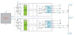
The drivers are suitable for mid- and high-power applications such as motor drivers for home appliances, factory automation, industrial drives and fans, UPSs, wireless chargers, and power-conversion and motor-driver inverters in industrial applications (Fig. 1).
The STGAP2GS is intended to drive enhancement-mode GaN FETs, thanks to its separate turn-on and turn-off output pins and to the optimized undervoltage-lockout (UVLO) protection. The gate driver offers 2-A current-source and 3-A current-sink capability plus rail-to-rail outputs. In addition, it’s driven by 3.3/5-V TTL/CMOS inputs with hysteresis. The STGAP2GS has separate sink and source pins for easy tuning of the gate-driving operation, and independent control with optimized turn-on and turn-off times via dedicated gate resistors.
Propagation delay across the 1,200-V isolation barrier is just 45 n, ensuring fast dynamic response. Furthermore, dV/dt transient immunity of ±100 V/ns over the full temperature range guards against unwanted transistor gate change.
The dual input pins allow for the selection of signal polarity control and implementation of HW interlocking protection to avoid cross-conduction in the event of controller malfunction. A standby mode is available to reduce idle power consumption.
Even basic devices such as a gate driver need design-in and applications support. In addition to the 20-page datasheet, ST offers two similar demonstration boards (Fig. 2): the EVSTGAP2GS for the STGAP2GS (SO-8 widebody package) and similar EVSTGAP2GSN for the STGAP2GSN (SO-8 narrow body package).
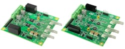
These boards combine either driver with ST’s SGT120R65AL 75-mΩ, 650-V enhancement-mode GaN transistors to help users evaluate the drivers’ capabilities. The board components are easy to access and modify to make their performance evaluation easier under different application conditions as well as enable fine adjustment of final application components.
Both the SO-8 wide-body STGAP2GS and the SO-8 narrow version STGAP2GSN are available now, priced from $1.42 for orders of 1,000 pieces.
About the Author

Bill Schweber
Contributing Editor
Bill Schweber is an electronics engineer who has written three textbooks on electronic communications systems, as well as hundreds of technical articles, opinion columns, and product features. In past roles, he worked as a technical website manager for multiple topic-specific sites for EE Times, as well as both the Executive Editor and Analog Editor at EDN.
At Analog Devices Inc., Bill was in marketing communications (public relations). As a result, he has been on both sides of the technical PR function, presenting company products, stories, and messages to the media and also as the recipient of these.
Prior to the MarCom role at Analog, Bill was associate editor of their respected technical journal and worked in their product marketing and applications engineering groups. Before those roles, he was at Instron Corp., doing hands-on analog- and power-circuit design and systems integration for materials-testing machine controls.
Bill has an MSEE (Univ. of Mass) and BSEE (Columbia Univ.), is a Registered Professional Engineer, and holds an Advanced Class amateur radio license. He has also planned, written, and presented online courses on a variety of engineering topics, including MOSFET basics, ADC selection, and driving LEDs.
Comment About the Article
To join the conversation, and become an exclusive member of Electronic Design, create an account today!

Leaders relevant to this article: