More Trusted Techniques to Lower EMI
This article is part of the TechXchange: Delving into EMI, EMC and Noise.
Members can download this article in PDF format.
Following on the previous article, here we’ll zero in on more tried-and-true electromagnetic-interference (EMI) reduction techniques for circuit and package designs that will help electrical/electronic designers pass EMI testing standards.
Dual Random Spread Spectrum (DRSS)
Dithering or spread-spectrum techniques have been used in radio and wired communications in the past. Switching power supplies, switching converters, and switch mode controllers all typically employ dual random spread spectrum (DRSS),1 a fairly new technique, to reduce EMI generated by switchers (for more, go here).
DRSS employs a digital algorithm that’s specifically created for spread spectral emissions within many different frequency bands. Performance will not have any tradeoff between these frequency bands.
Low EMI in Light Communications (LC)
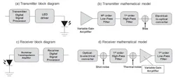
Light communications (LC), also known as LiFi (IEEE 802.11bb in progress), is an excellent method of wireless communication in the industry outside of the traditional wireless radio spectrum (Fig. 1).2 There exists access to a huge, globally unlicensed Li-Fi space. It has large bandwidth, good security, data density, and energy efficiency that will not be affected by, or contribute to, EMI under 3 THz in frequency.
Graphene Film Shielding
One form of shielding involves using an ultra-thin, flexible, and lightweight graphene film that can be employed via an easily applied vacuum evaporation method, which is followed up by a graphitization process.3
Graphitization is defined as the formation of graphite, a.k.a. free carbon, in low-alloy steel or iron, which may occur when their components become exposed to elevated temperatures for a long period of time. Graphitization is able to increase the orderly arrangement of carbon atoms that are organized into layers of crystalline structures.
This graphitization example in Reference 3 had an EMI shielding effectiveness (SE) of 43 dB in the frequency band of 8.2 to 12.4 GHz. The graphene film that was used had an ultra-thin thickness of 20 μm. Its specific EMI SE (SE/thickness) could reach as high as 2150 dB/mm. The graphene film also showed excellent flexibility and durability in a bending test.
Grounded Lid Aperture for Package-Level EMI Shielding
Lids are typically employed for an IC package to provide warpage control, die protection, and heat spreading. High-speed signals from a die and traces may be coupled to the IC lid, leading to radiated emissions that will result in EMI problems.
Methods to mitigate EMI involve connecting the IC package lid to the package ground via an electrically conductive adhesive. Some apertures on a grounded lid will be required to be left open for package reliability during the lid-attachment process. These apertures will decrease the SE of the grounded lid.
Discussed below is an equivalent model that’s used to examine the effectiveness of the aperture location, size, and number to reduce any radiated emissions from the grounded lid.4
Possible EMI and Reliability Issues in a Grounded Lid
Designers must carefully design the package lid because its location will typically be close to the electromagnetic (EM) noise source (die). This may easily excite radiated emissions from the lid and lead to EMI problems.
To ensure the reliability of a package during the lid attachment process and temperature cycling test, designers must implement some apertures in a grounded lid. This will help to release additional pressure caused by the expanded hot air inside the package.
However, any lid apertures will lead to a degradation of the SE of a grounded lid and likely result in some actual and potential EMI problems. To mitigate the EMI effects, the grounded lid design should be reconsidered from both a reliability and EMI perspective. The influence of some aperture parameters, such as their location, number, and size, are discussed below.
Modeling Grounded Lids
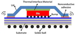
This grounded lid method shown in Figure 2 focuses on mechanical and thermal performance. Connecting the lid to the package plane is done with a strong sealant adhesive. Designers need to beware of higher frequencies within the package that may make the lid an EMI radiator.
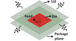
A traditional lid equivalent circuit model for EMI analysis is a patch antenna enclosed with a metal cover (Fig. 3). The noise source (die) is replaced by a patch antenna with a feed in the center. This enables noise to leak out from four sides of the lid directly. Some parallel plate resonances, excited unintentionally by the die, will further enhance the EMI problems.
In a grounded lid structure (Fig. 4), the lid is connected to ground via a conductive adhesive. Fortunately, this method makes the lid act as a Faraday cage, which leads to effective EMI shielding.
Package Reliability Concerns
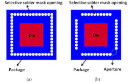
We also must consider package reliability by adding some apertures on the grounded lid (Fig. 5). The apertures are needed for package reliability during the process of attachment.
Noise will leak out from the apertures (Fig. 5b) and may affect other components in the design area and even beyond. The solution is to design optimum apertures to mitigate any radiation from the package. Reference 4 offers the best possible solution for the aperture location, number, and size that will effectively balance enhanced package reliability and reduced radiated emissions.
Summary
Minimizing EMI in electronic circuit designs is a very critical part of optimizing circuit performance. EMI emanating outward or impinging upon circuit designs can cause havoc, leading to errors in circuit performance as well as in any susceptible nearby circuitry. This article presented EMI reduction techniques to help eliminate this prevalent problem.
Read more articles in the TechXchange: Delving into EMI, EMC and Noise.
References
1. “EMI Reduction Technique, Dual Random Spread Spectrum,” Application Note, Paul Curtis and Eric Lee, Texas Instruments, 2022.
2. “Current Status and Challenges of Li-Fi: IEEE 802.11BB,” Evgeny Khorov and Ilya Levitsky, IEEE Communications Standards Magazine, June 2022.
3. “A flexible and ultrathin graphene film for electromagnetic interference shielding,” Wei Liu, Wenhua Wang, Kun Jia, Man Li, Donghong Wang, IEEE, 2021.
4. “Effects of Grounded-Lid Apertures for Package-Level Electromagnetic Interference (EMI) Shielding,” IEEE 2017.
About the Author

Steve Taranovich
Freelance Technical Writer, Phoenix Information Communication LLC
Steve is a contributing editor to Electronic Design.
Author of the non-fiction “Guardians of the Right Stuff,” a true story of the Apollo program as told by NASA and Grumman Corp. engineers, an astronaut, and technicians.
Experienced Editor-In-Chief of EETimes/Planet Analog and Senior Technical Editor at EDN running the Analog and Power Management Design Centers from 2012 to 2019.
A demonstrated history in electronic circuit design and applications for 40 years, and nine years of technical writing and editing in industry. Skilled in Analog Electronics, Space-related Electronics, Audio, RF & Communications, Power Management, Electrical Engineering, and Integrated Circuits (IC).
1972 to 1988 worked as a circuit design engineer in audio (8 years) and microwave (8 years). Then was Corporate Account Manager/applications engineer for Burr-Brown from 1988 to 2000 when TI purchased Burr-Brown. Worked for TI from 2000 to 2011.
Strong media and communication professional with a BEEE from NYU Engineering in 1972 and an MSEE from Polytechnic University in 1989. Senior Lifetime member of IEEE. Former IEEE Long Island, NY Director of Educational Activities. Eta Kappa Nu EE honor society member since 1970.
Voice Your Opinion!
To join the conversation, and become an exclusive member of Electronic Design, create an account today!

Leaders relevant to this article:


