GaN Overvoltage Effects: Degradation and Recovery
This article is part of the TechXchange: Gallium Nitride (GaN).
Members can download this article in PDF format.
What you'll learn:
- What's needed to fill in the gaps in understanding GaN HEMTs and their catastrophic failures.
- Degradation mechanisms that plague GaN HEMTs.
- Why overvoltage ruggedness and surge-energy withstand go hand-in-hand.
Gallium-nitride (GaN) high electron mobility transistors (HEMTs) have a limited avalanche capability. Thus, they may frequently experience catastrophic failures in voltage overshoot up to their dynamic breakdown voltage (BVdyn).1 Unfortunately, some very critical application-oriented knowledge gaps remain for the overvoltage ruggedness of GaN power HEMTs (Fig. 1).
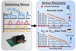
The ongoing activity of GaN power HEMT device recovery after an overvoltage stress and the recovery acceleration event are critical for device users; however, their recovery remains unknown. An appreciable change in internal carrier dynamics may occur in GaN power HEMTs at an overvoltage/surge approaching BVdyn.
For any given GaN HEMT device, a supplier must determine its potential use conditions ranging from manufacturing to shipping to the end-user. In addition, its exposure to environmental settings in its useful life (indoor and outdoor) must also be examined. System and application stress, and lifetime requirements, must be observed as well.
Subsequently, a failure modes and effects analysis (FMEA) will need to be created that combines the collected knowledge of device behaviors and possible (failure/degradation) effects when stress and other factors are considered. To aid in creation of the FMEA, JEDEC published JEP131 (“Potential Failure Mode and Effects Analysis–FMEA”).
GaN HEMT Degradation
GaN HEMTs can be influenced by various degradation mechanisms that aren’t observed in silicon or gallium-arsenide (GaAs) devices because of operating conditions under higher current densities, higher temperatures, and electric fields. Within such environments, GaN HEMTs may experience degradation with the possibility of catastrophic failures.
Material properties, like piezoelectric effects, occur with heteroepitaxy (this is a type of epitaxy performed with materials that differ from each other). In heteroepitaxy, a crystalline film is grown on a crystalline substrate or film of a different material. This technology is typically applied in cases where crystals can’t otherwise be obtained (to fabricate integrated crystalline layers of different materials) on silicon-carbide (SiC) or Si substrates, thermal interfaces with packages and substrates, and higher densities of deep-level defects.
Most of the degradation-related effects are able to be traced, measured, and analyzed by electrical performance testing. Nevertheless, as compared with the continuous degradation processes, catastrophic failures are instantaneous and difficult to analyze with common electrical measurements. Thus, more attention can be drawn by performance instability research and long-term reliability instead of physical analyses of post failures, which are significant in reliability improvements of GaN HEMTs.
The most stressful GaN test regimes are: 5,6,7
- Off-state: high vertical and lateral field (dielectric failure, GaN TBD)
- Hard-switching: self-heating and hot electrons
- On-state: positive gate, p-GaN, or gate dielectric degradation
Time-Dependent Dielectric Breakdown Issues
GaN devices have no dielectrics, but semi-insulating GaN behaves like a dielectric. Failures in GaN are Weibull-distributed.9
Time-dependent dielectric breakdown (TDDB), which is under constant voltage stress (CVS) of GaN power devices, are subjected to positive and negative substrate biases that have been evaluated experimentally. These experimental results, along with statistical analysis of GaN power devices’ TDDB under different substrate biases, have been studied.10
The Weibull shape parameter β will indicate if the failure rate is increasing, constant, or decreasing. Therefore, if β < 1, the system or component will have a decreasing failure rate. This kind of scenario is a typical sign of “infant mortality” and indicates whether the system or component is failing during its “burn-in” period. If β = 1, there will be a constant failure rate.
Less electron injection, from depleted two-dimensional electron gas (2DEG), will monotonically decrease of the shape parameter β from intrinsic breakdown (caused by electrical stress induced defect generation) to extrinsic breakdown (caused by defects induced by the manufacturing process).
Two different trap mechanisms, with decreased shape parameter β and increased scale parameter η, were observed under positive substrate biases. The statistical parameters of progressive breakdown were collected, which indicate that the creation of a percolation path of GaN power devices under substrate biases strongly depends on dielectric material itself, while the trap generation process relates to GaN buffer traps induced from deep-level traps.
Examining Overvoltage Ruggedness of P-Gate GaN HEMTs
The definition of essential ruggedness of power devices is the capability to safely withstand any surge energy. The surge ruggedness of the GaN HEMT, which has no or minimal avalanche capability, hasn’t been fully understood to date. To help better comprehend it, thorough physics were applied to the surge-energy withstand process and the failure mechanisms of p-gate GaN HEMTs.12
With the qualification of GaN power HEMTs, we must consider the device ruggedness against any out-of-SOA (safe operating area) events. The key factor in power-device robustness is the ability to safely withstand surge energy. This capability is needed in many power applications, which include automotive systems, power grids, and more.
A widely used method to characterize a device’s surge-energy capability is the unclamped inductive switching (UIS) (Fig. 2).
The surge-energy withstand capability of GaN HEMTs isn’t fully clear, mostly because the GaN HEMT is a power device that has no, or extraordinarily little, avalanche capability. This differs from Si and SiC MOSFETs, because no inherent p-n junctions are connected between the source and drain in GaN HEMTs.
Therefore, the holes generated during impact ionization and multiplication can’t be effectively extracted. This limits the device’s capability to accommodate the high current from unclamped inductive loads at high Vds. The lack of avalanche capability might suggest a different surge-energy withstand dynamic within GaN HEMTs.
Surge-Energy Withstand Process
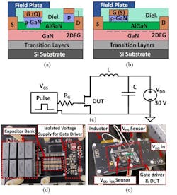
Reference 11 unveils the withstand process and failure mechanisms of commercial p-gate GaN HEMTs, which are under transient surge energy and overvoltage. It’s implemented by a traditional UIS test coupled with a clamped inductive switching circuit that has a controlled parasitic inductance.
The surge-energy withstand process and failure mechanisms of GaN HEMTs are radically different from the Si and SiC MOSFETs with their avalanche capability. The GaN HEMT can withstand surge energy through its intrinsic overvoltage ability. However, it’s not able to dissipate the surge energy during the withstand process.
The device failure, under surge energy, is mostly related to the peak overvoltage, but it isn’t sensitive to dV/dt or duration of the surge voltage. The magnitude of surge energy is no longer a parameter that can directly reflect the device’s intrinsic surge ruggedness for GaN HEMTs. The main failure mechanism is partly E-field limited and the breakdown locations in the device will be consistent with the peak E-field locations.
Read more articles in the TechXchange: Gallium Nitride (GaN).
References
1. “Degradation and Recovery of GaN HEMTs in Overvoltage Hard Switching Near Breakdown Voltage,” IEEE Transactions on Power Electronics, Vol. 38, No. 1, January 2023.
2. “Progress and Current Topics of JEDEC JC-70.1 Power GaN Device Quality and Reliability Standards Activity,” IEEE.
3. “Recent progress of physical failure analysis of GaN HEMTs,” Journal of Semiconductors, 2021.
4. Recent progress of physical failure analysis of GaN HEMTs (PDF).
5. Product-level Reliability of GaN Devices.
6. “GaN Power Device Reliability,” Dr. Douglas J. Sheldon, California Institute of Technology, 2018. Government sponsorship acknowledged.
7. “Failure modes and mechanisms of GaN HEMTs for microwave and power applications”, E. Zanoni, et.al, IRPS, 2019.
8. “Improving Reliability for GaN and SiC, Semiconductor Engineering,” Mark Lapedas, 2020.
9. “Experimental Demonstration of Weibull Distributed Failure in p-type GaN High Electron Mobility Transistors under high forward bias stress,” Proceedings of the 2016 28th International Symposium on Power Semiconductor Devices and ICs (ISPSD), June 12-16, 2016, Prague, Czech Republic.
10. “Experimental Evaluation of Time-Dependent Dielectric Breakdown for GaN MIS HEMTs under Various Substrate Biases,” IEEE, 2019.
11. Weibull.com.
12. “Surge-Energy and Overvoltage Ruggedness of P-Gate GaN HEMTs, IEEE Transactions on Power Electronics,” Vol. 35, No. 12, December 2020.
About the Author

Steve Taranovich
Freelance Technical Writer, Phoenix Information Communication LLC
Steve is a contributing editor to Electronic Design.
Author of the non-fiction “Guardians of the Right Stuff,” a true story of the Apollo program as told by NASA and Grumman Corp. engineers, an astronaut, and technicians.
Experienced Editor-In-Chief of EETimes/Planet Analog and Senior Technical Editor at EDN running the Analog and Power Management Design Centers from 2012 to 2019.
A demonstrated history in electronic circuit design and applications for 40 years, and nine years of technical writing and editing in industry. Skilled in Analog Electronics, Space-related Electronics, Audio, RF & Communications, Power Management, Electrical Engineering, and Integrated Circuits (IC).
1972 to 1988 worked as a circuit design engineer in audio (8 years) and microwave (8 years). Then was Corporate Account Manager/applications engineer for Burr-Brown from 1988 to 2000 when TI purchased Burr-Brown. Worked for TI from 2000 to 2011.
Strong media and communication professional with a BEEE from NYU Engineering in 1972 and an MSEE from Polytechnic University in 1989. Senior Lifetime member of IEEE. Former IEEE Long Island, NY Director of Educational Activities. Eta Kappa Nu EE honor society member since 1970.
Comment About the Article
To join the conversation, and become an exclusive member of Electronic Design, create an account today!

Leaders relevant to this article: