Bringing Isolation, High Efficiency, and Lower Noise to Switching Power Supplies
This article is part of the TechXchange: Delving into EMI, EMC and Noise.
Members can download this article in PDF format.
What you'll learn:
- Methods for mitigating noise in SMPS.
- Creating lower-noise designs.
- Challenges encountered with conducted emissions and meeting emissions standards.
Power designers in search of high power efficiency in step-up and step-down conversion with switching power supplies need to minimize DC-DC power converter EMI noise. This article will provide some unique EMI noise mitigation solutions.
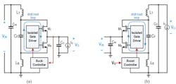
Isolated DC-DC bias converters provide isolated communication and sensing via bias power across the isolation barrier. Current/voltage sensors, gate drivers, and digital isolators usually require power that can range from less than 15 W to as little as tens of milliwatts (Fig. 1).1
Examining Noise-Spreading Effects in Switched-Mode Power Supplies
Switched-mode power supplies (SMPS) have numerous advantages versus linear power supplies. They include higher efficiency, lower weight, smaller physical size, and the ability to boost the output voltage above the input voltage. However, there’s one major disadvantage—noise.2
Switching power regulators, by their design, produce large dv/dt and di/dt. This leads to a possible, pesky noise problem: interference from nearby circuitry, systems, and devices. Designers may first employ some of these methods to mitigate that noise:
- Slow down the switching frequency transitions.
- Minimize the high di/dt current loop areas.
- Snub the high dv/dt nodes.
- Select a switching frequency that will least disturb the system.
When all else fails, designers might want to consider a technique known as spread-spectrum frequency dithering (SSFD). With SSFD, the switching frequency will be swept within a limited range around a nominal set point.
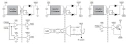
EMI is always causing switching power-circuitry design problems due to common-mode (CM) noise present in the design. Many commonly known methods can help minimize the CM noise that flows through the LISN (Fig. 2).
The line impedance stabilization network (LISN) provides the following:
- A stable line source impedance
- A safe connection of measuring equipment
- The isolation of the power-source noise
- The “total” noise levels that are measured separately in L1 and L2
- Termination into a 50-Ω load that can be internal to an EMI receiver
In essence, the LISN is a high-pass filter. The high-frequency noise gets trapped via the LISN capacitor and the amplitude gets measured based on the voltage across the 50-Ω load, which in this case is inside the EMI receiver in Figure 2.
Designing for Noise Mitigation
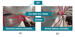
At first glance, designers may explore methods of noise reduction: careful selection of components; choosing a PCB layout that will best help mitigate noise; grounding; shielding; isolation; input/output filtering; separating noisy components to areas away from more sensitive components; and choosing the best shielded cable design (Fig. 3).3
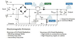
Power designers must pay careful attention to the loop area corresponding with the input-current path leading to a switching regulator. This can have a major impact on reducing any pesky radiated emissions.
Next, designers should consider component selection, which is a crucial factor in EMI mitigation. If we look at Figure 1, we might want to look closely at the parasitic heatsink capacitance (Cphs). This capacitance, as well as various other output-stage impedances, could compromise any conducted and radiated emissions when they perform with a high output-stage current and voltage slew rates.
Challenges Dealing with Conducted Emissions
Class A and Class B limits for EN 55022/32 conducted emissions, with quasi-peak and average signal detectors, span a frequency range from 150 kHz to 30 MHz. Both quasi-peak and average limits need to be satisfied. The EN 55022 Class B QP (quasi-peak) conducted-emissions limit is 60 dBmV at 10MHz.
The Comité International Spécial des Perturbations Radioélectriques (CISPR) 32 standard dictates the maximum conducted emissions and radiated emissions for industrial equipment. It defines two classes of equipment that are associated with the end-user environment:
- Class B requirements are intended to give satisfactory protection to broadcast services in residential environments. Equipment that’s planned primarily for residential environments must meet Class B limits (all broadcast receiver equipment is considered as Class B).
- Class A requirements will cover all non-Class B equipment; Class A-compliant equipment complies with more flexible class limits.4,5
Meeting Radiated Emission Standards
All equipment that must meet radiated-emissions standards gets tested within a Faraday shield chamber. The test chamber is typically 10 meters long. There are acceptable 3-m chambers as well, which have higher limits to account for a higher emissions strength difference in scale (Fig. 4).
Usually, the SMPS will have a clock that runs below 1 GHz. Higher frequency limits would not apply unless the equipment being used has a clock which runs at greater than 1 GHz, such as in a personal computer.
Read more articles in the TechXchange: Delving into EMI, EMC and Noise.
References
1. “Power through the isolation barrier: The landscape of isolated DC/DC bias power supplies,” Ryan Manack, Texas Instruments, 2021.
2. “Understanding Noise-Spreading Techniques and their Effects in Switch-Mode Power Applications,” Texas Instruments, 2011.
3. “Fundamentals of EMI Requirements for an Isolated DC/DC Converter,” R. Martinez, Z. Zhang, 2021.
4. “PR102554 Texas Instruments CE Mark Report Rev. 1,” National Technical Systems, Electromagnetic Compatibility (EMC) Requirements EN55032 Test Report for UCC12050, CISPR 32 Radiated and Conducted Emissions Certification Report, September 2019.
5. Daniel Hoolihan, www.interferencetechnology.com.
6. “Introduction to EMI in Power Supply Designs, Isolated Gate Drivers,” Bing Lu, High Voltage Seminar, Texas Instruments.
7. “An overview of conducted EMI specifications for power supplies,” Timothy Hegarty, Texas Instruments, 2018.
About the Author

Steve Taranovich
Freelance Technical Writer, Phoenix Information Communication LLC
Steve is a contributing editor to Electronic Design.
Author of the non-fiction “Guardians of the Right Stuff,” a true story of the Apollo program as told by NASA and Grumman Corp. engineers, an astronaut, and technicians.
Experienced Editor-In-Chief of EETimes/Planet Analog and Senior Technical Editor at EDN running the Analog and Power Management Design Centers from 2012 to 2019.
A demonstrated history in electronic circuit design and applications for 40 years, and nine years of technical writing and editing in industry. Skilled in Analog Electronics, Space-related Electronics, Audio, RF & Communications, Power Management, Electrical Engineering, and Integrated Circuits (IC).
1972 to 1988 worked as a circuit design engineer in audio (8 years) and microwave (8 years). Then was Corporate Account Manager/applications engineer for Burr-Brown from 1988 to 2000 when TI purchased Burr-Brown. Worked for TI from 2000 to 2011.
Strong media and communication professional with a BEEE from NYU Engineering in 1972 and an MSEE from Polytechnic University in 1989. Senior Lifetime member of IEEE. Former IEEE Long Island, NY Director of Educational Activities. Eta Kappa Nu EE honor society member since 1970.
Comment About the Article
To join the conversation, and become an exclusive member of Electronic Design, create an account today!

Leaders relevant to this article: