Miniature Power MOSFETs Thrive in Tight Spaces

This article is part of the TechXchange: Power Supply Design.
To succeed in the world of power electronics, all it takes is a little silicon—literally.
To prove it, power semiconductor companies are packing low-voltage MOSFETs into smaller easy-to-cool packages that are scarcely larger than a grain of rice and ideal for everything from industrial to consumer devices.
To boost power density, they’re ushering in improvements across the board. New types of packaging, including power quad flat no-lead (PQFN) and enhanced chip-scale packages (CSP) with minuscule form factors, are rolling out to reduce parasitic elements (resistance, inductance, and capacitance) that can drive excess power losses. Limiting these parasitics also inevitably reduces heat that can sap a system’s performance.
Improvements to the trench gate and other internal building blocks of the power MOSFETs are relevant, too. These innovations play a role in reducing power losses due to the on-resistance (RDS(on)) and drain current as well as switching losses that happen when the FET turns on and off. The result is higher power efficiency, which in turn works to prevent heat from building up in the FET, package, and system.
Typically operating at relatively tame voltages of less than 100 V, these mini MOSFETs are a fit for load switches and synchronous rectification in switched-mode power supplies (SMPS) in servers, telecom, and portable and wireless chargers. They’re also ideal for protecting the battery packs in smartphones during charging and discharging, ORing power systems, or controlling very small brushless DC (BLDC) motors.
While new semiconductors such as gallium nitride (GaN) are raising the bar for power density and switching frequency at high voltages, companies still have levers to pull to prolong the dominance of silicon at lesser voltages.
The Impact of Packaging on Power MOSFETs
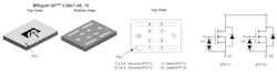
Packaging innovation is a key strategy at Alpha and Omega Semiconductor (AOS), which is loading its latest mini MOSFETs into a more mechanically robust CSP called MRigidCSP (Fig. 1).
The company is using the more robust CSP package for the first time in its latest 12-V common-drain, dual-channel MOSFET, the AOCR33105E, targeted at fast-charging batteries in smartphones and PCs. With a source voltage (VSS) of 12 V and gate-to-source (VGS) voltage of 8 V, the discrete power device fits in a compact footprint of 2.08 × 1.45 mm and reduces source-to-source resistance (RSS) to less than 3 mΩ at 4.5 V.
Fast charging, which requires minimal power loss in the battery-management circuitry, is widely used in portable devices. As charging currents increase, ultra-low resistance is needed to improve performance.
Safely charging and discharging the battery in a consumer device requires a bidirectional switch, a type of component also commonly used to protect the battery from unforeseen damage. A bidirectional switch is usually formed by combining a pair of MOSFETs—one to control the current in one direction and another to control its flow in the opposite direction. The parts tend to be placed back-to-back in a common-source or a common-drain configuration to block high currents from traveling through the discrete power device.
In a standard wafer-level chip-scale package (WL-CSP), the substrate accounts for a large portion of the total resistance when the FETs are connected to each other for battery management. A thinner substrate translates into less resistance, but it also drastically reduces the robustness of the package, according to the company. The lack of mechanical stability can stress out the FET when it comes time to attach it to a PCB. Stress raises the risk of warping or cracking in the silicon die—and can lead to failures in the field.
Based on its latest trench-power MOSFET, the part features ultra-low on-resistance with electrostatic-discharge (ESD) protection to improve performance and safety when used as a building block in a battery-management system—in a protection switch or in mobile battery charging and discharging circuits. AOS said the AOCR33105E is currently in mass production. Pricing for the components starts at $0.405 each in 1,000-unit quantities.
How to Limit Losses in Power MOSFETs
ROHM Semiconductor unveiled a new series of power MOSFETs targeting 24-, 36-, and 48-V power supplies used in everything from base stations and data centers to industrial and consumer motor drives.
In general, power FETs are characterized by two main parameters leading to excess power losses:
- On-resistance (RDS(on)): The resistance value between the drain and source while the MOSFET is turned on, which directly impacts power loss during conduction.
- Gate-drain charge (QGD): The amount of charge when charging the capacitance between the gate and drain after the MOSFET turns on, which directly impacts the switching speed of the power device. Faster switching equals better switching loss.
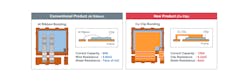
The problem is that the on-resistance of the MOSFET is inversely proportional to the die area of the device, while the gate-drain charge increases proportionally depending on the die area. Thus, it’s challenging to improve one characteristic without compromising the other. The company is navigating the tradeoff by using copper clip connections instead of the standard "ribbon" bonding and improving the construction of the internal gate in the power MOSFET (Fig. 2).
ROHM said the RS6xxxxBx and RH6xxxxBx series raise the bar for power efficiency. They deliver around 50% less RDS(on) at 2.1 mΩ than the competition while occupying 5.0- × 6.0- × 1.0-mm HSOP8 or 3.3- × 3.3- × 0.8-mm HSMT8 packages that use copper clip connections to limit the package resistance and increase current capacity to 120 A. Improvements to the internal construction of the gate reduce QGD—typically a tradeoff with the RDS(on)—by 40% at 60 V, the company said.
With breakdown voltages of 40 to 150 V, the switches are said to deliver peak efficiency of over 95% in the output current range during steady-state operation when used in industrial-grade power supplies.
Packing More MOSFET into the QFN Package
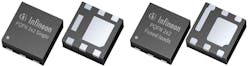
Infineon Technologies is packing more of its OptiMOS power MOSFET family into smaller PQFN packages that measure a mere 2 × 2 mm, substantially increasing power density (Fig. 3).
The new OptiMOS 6 40-V and OptiMOS 5 25- and 30-V power MOSFETs support very low RDS(on) with high figures of merit to enhance dynamic switching operation. That includes gate charge (QG), or the total amount of charge that must be pumped into the gate to turn on the switch. The improved output charge (QOSS) helps reduce power loss from charging and discharging the output capacitance during switching.
The smaller the package, the more difficult it is for the device to dissipate its heat. Unless special attention is paid to removing heat from the FET and getting it out of the package, overheating can occur. While it upgraded the silicon under the hood to cut power losses, Infineon also improved the packaging with a reinforced clip that reduces parasitics and junction-case thermal resistance (Rthj-c, max = 3.2 K/W) for better cooling.
The reliability of the enhanced PQFN package reduces the need for paralleling, giving customers another way to save space and reduce costs in switch-mode or other power supplies, said Infineon.
The small footprint and flexible pinouts facilitate placement of the new MOSFETs and supplemental components on a PCB in cases where form factor and geometric outline are key obstacles, according to the company.
The more compact 40-V OptiMOS 6 MOSFET with RDS(on) of 5.7 mΩ and the OptiMOS 5 MOSFETs that operate at 25 V and 30 V with RDS(on) of 2.4 mΩ and 3.6 mΩ, respectively, are currently shipping.
This article is part of the TechXchange: Power Supply Design.
About the Author

James Morra
Senior Editor
James Morra is the senior editor for Electronic Design, covering the semiconductor industry and new technology trends, with a focus on power electronics and power management. He also reports on the business behind electrical engineering, including the electronics supply chain. He joined Electronic Design in 2015 and is based in Chicago, Illinois.
Comment About the Article
To join the conversation, and become an exclusive member of Electronic Design, create an account today!

Leaders relevant to this article: