This Week in PowerBites: Smart IGBTs, Doubling Down on Grid-Scale Storage

This article is part of the This Week in PowerBites Library Series.
National Lab Sets Its Sights on Changing the Economics of Grid-Scale Storage

To further accelerate its efforts in developing advanced grid-scale energy storage technologies, Pacific Northwest National Laboratory-Richland (PNNL) added a new major facility on its campus called the Grid Storage Launchpad (GSL). Scheduled to open in 2024, the GSL is funded by the Department of Energy’s (DoE) Office of Electricity (OE) with a mission to support development of large-scale energy-storage technologies that provide increased reliability and lower cost.
The GSL facility's goal is speed up development and deployment of next-generation grid storage technologies through systematic and independent validation—from basic materials and components to prototypes that enable safer, more cost-effective, and more durable technologies. Strategic funding from the State of Washington, Battelle, and PNNL provide further support for GSL equipment and R&D activities that complement the DoE OE investment.
Although lithium-ion has been a favorite for a long time, PNNL researchers are studying different kinds of materials, such as sodium ion, nickel iron, or lead acid, that could be scaled up to cost-effectively provide electricity for longer periods of time for the grid—a concept known as long-duration energy storage. Testing these new technologies helps optimize performance, which is critical for commercialization and eventual public adoption.
At GSL, researchers will be able to increase the number of tests performed as well as the size of battery that can be tested.
PNNL says that research in the new facility will complement the work being done across the street at the Electricity Infrastructure Operations Center, where PNNL researchers are developing new ways to improve the resiliency of the country’s vast electrical grid.
In addition to technology development and evaluation, GSL's mission also includes fostering collaboration between national labs and other stakeholders to support OE’s mission, the Energy Storage Grand Challenge, and the Long Duration Storage Shot, a project aimed at delivering 10+ hours of storage at 90% of today’s cost within the next decade.
“GSL will allow us to take new technologies from development of basic materials to testing of 100-kW systems under real-world conditions,” said Vince Sprenkle, an advisor at PNNL who leads the PNNL’s energy storage research efforts. “Energy storage is needed to improve resilience and reliability in a decarbonized energy system, and GSL will get us there.”
GaN Devices Combine Power, Drive, Sensing, and Protection in Single Cool-Running Package

Navitas Semiconductor introduced its 4th-generation gallium-nitride (GaN) technology, intended to support the demanding requirements of high-power applications in data centers, solar/energy storage and electric-vehicle markets, where efficiency, power density, and robust and reliable operation are critical.
Manufactured in Hsinchu, Taiwan by long-term Navitas partner TSMC, GaNFast power ICs integrate GaN power and drive, with control, sensing, and protection to enable faster charging, higher power density, and greater energy savings. Now, the new the new 4th-generation GaNSafe platform has been engineered with additional, application-specific protection features, functions, and new high-power packaging to deliver enabling performance under grueling high-temperature, long-duration conditions.
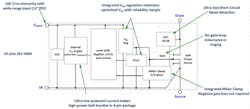
The initial, high-power 650/800-V GaNSafe portfolio covers a range of on-resistance (RDS(on)) from 35 to 98 mΩ in a novel, robust, and cool-running surface-mount TOLL package, to address applications from 1,000 to 22,000 W. GaNSafe integrated features and functions include:
- Protected, regulated, integrated gate-drive control, with zero gate-source loop inductance for reliable, high-speed, 2-MHz switching capability to maximize application power density.
- High-speed short-circuit protection, with autonomous “detect and protect” within 50 ns—4X faster than competing discrete solutions.
- Electrostatic-discharge (ESD) protection of 2 kV, compared to zero for discrete GaN transistors.
- 650-V continuous and 800-V transient-voltage capability to aid survival during extraordinary application conditions.
- An easy-to-use, complete, high-power, high-reliability, high-performance power IC with only four pins to help accelerate customer designs.
- Programmable turn-on and turn-off speeds (dV/dt) to simplify EMI regulatory requirements.
Note: It's important to remember that all of these features are integrated into the same GaN die that holds the power devices—they’re not "integrated" by co-packaging several different devices. Besides reducing cost and PCB footprint, this improves the devices' protection speed and transient response time.
Unlike discrete GaN transistor designs, with voltage spikes, undershoot, and specification breaches, GaNSafe delivers an efficient, predictable, reliable system. GaNSafe’s robust 4-pin TOLL package has achieved the tough IPC-9701 mechanical reliability standard. It delivers simple, strong, dependable performance as compared to multichip modules that require 3X as many connections and have poor cooling capability.
Navitas’ market-specific system design centers offer complete reference designs for selected applications. Examples of system platforms enabled by GaNSafe technology include:
- The CRPS185 data-center power platform. It delivers a full 3,200 W of power in only 1U (40 mm) × 73.5 mm × 185 mm (544 cc), achieving 5.9 W/cc or almost 100 W/in.3 power density. This is a 40% size reduction vs. the equivalent legacy silicon approach and reaches over 96.5% efficiency at 30% load. It also maintains over 96% stretching from 20% to 60% load, creating a “Titanium Plus” benchmark.
- The company’s 6.6-kW, 3-in-1 bidirectional EV onboard charger (OBC) with 3-kW DC-DC. This 96%+ efficient unit has over 50% higher power density, and with efficiency over 95%, delivers up to 16% energy savings as compared to competing solutions.
Also check out the company’s complementary GeneSiC silicon-carbide power devices.
Automotive-Grade, High-Voltage Hall ICs Target Magnetic Detection

The BD5310xG-CZ/BD5410xG-CZ Hall ICs developed by ROHM Semiconductor are designed for automotive applications requiring magnetic detection of proximity, position, and rotation. Typical applications include door locks, seat position, seat belts, wiper motors, power windows, sliding doors, etc.
According to the company, its advanced design and manufacturing processes give the devices enhanced reliability and an industry-leading 42-V withstand voltage that enables direct connection to a primary (12-V battery) power supply. This contributes to improved reliability under battery power, which can fluctuate rapidly depending on the operating conditions.
In addition, all devices in the series feature a wide operating supply voltage range of 2.7 to 38 V. The sensors' unique internal topology also reduces power consumption to 1.9 mA, approximately 20% lower than most other comparable products. Both series comply with the AEC-Q100 (Grade 1) automotive reliability standard, while incorporating multiple protection circuits required for vehicle systems.
The BD5310xG-CZ series is a unipolar detection type, while the BD5410xG-CZ series provides latch-type detection, giving designers the flexibility to select the ideal product based on set needs. A total of 11 models are offered in detection magnetic flux densities, ranging from 2.0 to 28.0 mT. Unipolar detection can be used to detect position in applications such as door open/close and door locks, whereas latch detection is well-suited for rotation detection in various motors used in power windows, sliding doors, etc.
Additional information is available at: BD53103G-CZTL, BD53108G-CZTL, and BD54102G-CZTL.
600-V-Rated "Intelligent" Power Devices Blend Power, Protection, and Control for BLDCs
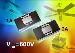
Toshiba Electronics Europe launched two products for brushless DC (BLDC) motor-drive applications such as fan motors, ventilation fans, air conditioners, air cleaners, and pumps. Each of the intelligent power devices (IPDs) incorporate 600-V-rated IGBTs and a matched gate driver as a one-chip solution in a single compact package. The output DC current (IOUT) rating of the TPD4163F is 1 A while the TPD4164F is rated at 2 A.
The two devices (TPD4163F and TPD4164F) have an IGBT saturation voltage (VCEsat) of 2.6 V and 3.0 V, respectively, while the diode forward voltage (VF) is 2.0 V and 2.5 V.
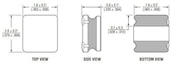
Both devices are housed in a miniature surface-mount HSSOP31 package. With dimensions of 17.5 × 11.93 × 2.2 mm, the PCB footprint is reduced by around 63% when compared with Toshiba’s existing DIP26 package products.
Both IPDs provide an additional advantage in geographic regions where supply voltage may fluctuate significantly due to instabilities in the local grid. To improve reliability under these conditions, the supply voltage rating (VBB) has been increased from 500 V to 600 V to introduce more design margin.
To support the new devices, Toshiba developed a reference design for a sensorless BLDC motor drive utilizing the new TPD4164F and a microcontroller (TMPM374FWUG).
Automotive-Grade, Semi-Shielded Power Inductors are AEC-Q200 Compliant
Five new members were added to Bourns’ AEC-Q200-compliant, semi-shielded power inductor product line. The SRN2010BTA, SRN2510BTA, SRN3010BTA, SRN3012BTA, and SRN3015BTA offer enhanced reliability due to their bottom-soldered lead-wire construction that boosts mechanical strength and stability.
These benefits, along with the inductors' multiple available footprints, makes them well-suited for differential-choke power-conversion solutions for automotive systems, DC-DC converters, and power supplies in consumer, industrial, and telecom electronics that frequently require high reliability. The semi-shielded design combines the benefits of both non-shielded and shielded inductors. This structure provides lower magnetic field radiation compared to non-shielded inductors and is a more cost-effective alternative to fully shielded ferrite-based inductors.
High-Current, High-Accuracy LDO Addresses Noise-Sensitive Power-Conversion Apps

Delivering a clean supply, the AP7179D is a 3-A-rated low-dropout (LDO) voltage regulator that supports 4.4-µVRMS operation (at 0.8-V output). The highly optimized device developed by Diodes Inc. will be used to power noise-sensitive components, such as the high-performance SerDes, RF devices, and data converters in high-speed communications, test and measurement, medical, and video applications.
The LDO's exceptional low-noise characteristics suit it for applications such as remote radio units (RRUs), outdoor backhaul units, mMIMO active antenna systems, ultrasound scanners, radar systems, and lab/field instrumentation.
The AP7179D has a ±1% output accuracy across line, load, and temperature. Its 180-mV (maximum) dropout voltage at a 3-A load current supports a wide voltage-conversion range. A low-noise reference and error amplifier enables a minimal noise floor. In addition, its 40-dB power-supply rejection ratio (PSRR) at 500 kHz substantially lowers the coupling of input supply noise to the output.
The LDO has an adjustable voltage output that can be set two different ways: via its pin-programmable mode between 0.8 and 3.95 V, or adjusted using an external resistor divider from 0.8 to 5.5 V. The resulting flexibility significantly reduces the number of accompanying components needed.
The device’s low output noise mitigates both power-supply-generated phase noise and clock jitter. As a result, alongside its high-current capabilities, this device is compatible with high-performance processors, such as FPGAs, ASICs, and DSPs.
The AP7179D comes in a compact, 20-pin W-QFN3535 (Type A1) package, and costs $0.70 in 1,000-unit quantities.
Advanced 650-V TRENCHSTOP IGBTs Address Energy-Efficient Power Applications
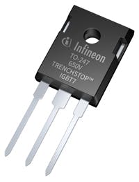
Infineon Technologies added a series of discrete 650-V IGBTs to its 7th-generation TRENCHSTOP IGBT family. The devices feature a cutting-edge EC7 co-packed diode with an advanced emitter-controlled design, coupled with high-speed switching capabilities that address the growing need for highly efficient power solutions in eco-friendly products. Using the latest micro-pattern trench technology, the TRENCHSTOP IGBT7 H7 offers excellent control and performance, resulting in significant loss reduction, improved efficiency, and higher power density.
Thus, the device will find homes in applications such as solar string inverters, energy-storage systems (ESS), electric-vehicle charging, and industrial UPS and welding.
The 650-V TRENCHSTOP IGBT7 H7 can deliver up to 150 A. The portfolio includes variants from 40 to 150 A, offered in four different discrete package types: TO-247-3 HCC, TO-247-4, TO-247-3 Plus, and TO-247-4 Plus. The TO-247-3 HCC variant of the TRENCHSTOP IGBT 7 H7 features a high creepage distance.
The TO-247 4-pin packages (standard: IKZA, Plus: IKY) are aimed at improving performance—they not only reduce switching losses, but also offer additional benefits such as lower voltage overshoot, minimized conduction losses. and very low reverse-current loss. With these features, the TRENCHSTOP IGBT 7 H7 help simplify design and minimizes the need to connect devices in parallel.
In addition, the IGBT features robust moisture resistance for reliable operation in harsh environments. The device is qualified for industrial use according to the relevant tests of JEDEC47/20/22, especially HV-H3TRB, suiting it for outdoor applications. Designed to meet the demand for green and efficient power applications, the device can be an ideal complement for the NPC1 topology often used in solar and ESS setups.
The TRENCHSTOP IGBT 7 H7 can be ordered now; qualification samples are available. For more information, go to www.infineon.com/discreteigbt7.
Rugged Battery-Management MOSFETs Feature Advanced Packaging for Lower Losses, Longer Life

MRigidCSP packaging technology developed by Alpha & Omega Semiconductor (AOS) has its sights set on battery-management applications. Designed to decrease on-resistance while increasing mechanical strength, MRigidCSP is currently offered on the AOCR33105E, a 12-V common-drain dual N-channel MOSFET. The robust package technology is particularly suited to battery applications in smartphones, tablets, and ultra-thin notebooks.
Fast charging, which requires lower power loss in the battery-management circuit, is now widely adopted for portable devices. As the charging currents increase, ultra-low electrical resistance is needed to prevent internal heating from damaging the device's cells.
In standard wafer-level chip-scale packages (WL-CSPs), the substrate can be a significant portion of the total resistance when back-to-back MOSFETs are employed in battery-management applications. A thinner substrate reduces the overall resistance but can drastically reduce the package’s mechanical strength. In turn, that can lead to more stress during the PCB assembly reflow process, potentially causing warping or cracking in the die and, ultimately, failure in the application.
The new device is designed with the latest trench-power MOSFET technology in a common drain configuration for design simplicity. It features ultra-low on-resistance with ESD protection to improve performance and safety in battery management, such as protection switches and mobile battery charging and discharging circuits.
The AOCR33105E in the MRigidCSP package is immediately available in production quantities with a lead time of 14-16 weeks. RoHS 2.0 compliant and halogen-free, it’s priced at $0.405 in 1,000-piece quantities.
Read more articles in the This Week in PowerBites Library Series.
About the Author

Lee Goldberg
Contributing Editor
Lee Goldberg is a self-identified “Recovering Engineer,” Maker/Hacker, Green-Tech Maven, Aviator, Gadfly, and Geek Dad. He spent the first 18 years of his career helping design microprocessors, embedded systems, renewable energy applications, and the occasional interplanetary spacecraft. After trading his ‘scope and soldering iron for a keyboard and a second career as a tech journalist, he’s spent the next two decades at several print and online engineering publications.
Lee’s current focus is power electronics, especially the technologies involved with energy efficiency, energy management, and renewable energy. This dovetails with his coverage of sustainable technologies and various environmental and social issues within the engineering community that he began in 1996. Lee also covers 3D printers, open-source hardware, and other Maker/Hacker technologies.
Lee holds a BSEE in Electrical Engineering from Thomas Edison College, and participated in a colloquium on technology, society, and the environment at Goddard College’s Institute for Social Ecology. His book, “Green Electronics/Green Bottom Line - A Commonsense Guide To Environmentally Responsible Engineering and Management,” was published by Newnes Press.
Lee, his wife Catherine, and his daughter Anwyn currently reside in the outskirts of Princeton N.J., where they masquerade as a typical suburban family.
Lee also writes the regular PowerBites series.
Comment About the Article
To join the conversation, and become an exclusive member of Electronic Design, create an account today!

Leaders relevant to this article: