This Week in PowerBites: SiC MOSFETs/Modules Plus Hybrid-Electric Aircraft’s First Test Flight

This article is part of the This Week in PowerBites Library Series.
First Test Flight of Hybrid-Electric Aircraft Shows Carbon-Alternative Promise

Could hybrid-electric aircraft help significantly reduce the carbon footprint of commercial aviation? The data collected from the first all-up test flight of EcoPulse, a hybrid-electric distributed propulsion aircraft demonstrator jointly developed by Daher, Safran, and Airbus, indicates that the concept works well and has potential as a practical alternative to today's turboprop fleets.
Based on a Daher TBM aircraft platform, the EcoPulse demonstrator can be flown using either its original turbine engine or a set of six integrated electric thrusters or e-Propellers (supplied by Safran), distributed along the wings. The plane's electric propulsion system integrates two power sources: a turbogenerator, i.e., an electric generator driven by a gas turbine (supplied by Safran), and a high-energy-density battery pack (supplied by Airbus).
At the heart of this architecture is a power distribution and rectifier unit (PDRU), responsible for protecting the high-voltage network and for distributing the available electrical power, as well as high-voltage power harnesses (both provided by Safran). The battery pack designed by Airbus is rated at 800 V DC and can deliver up to 350 kW of power.
EcoPulse’s first flight in its hybrid mode occurred on November 29, marking the culmination of several technical milestones, including extensive ground tests and 10 hours of flight tests of the aircraft with the electrical systems inactive. During the 100-minute flight, the crew engaged the electric propellers for the first time and verified the proper functioning of the demonstrator's flight control computer, high-voltage battery pack, distributed electric propulsion, and hybrid electric turbogenerator.
Unveiled at the 2019 Paris Air Show, EcoPulse is one of the major collaborative projects in Europe in the field of aviation decarbonization. It’s supported by CORAC (the French Civil Aviation Research Council), and co-funded by DGAC (the French Civil Aviation Authority) through France Relance (the French government’s economy recovery plan) and NextGeneration EU.
The demonstrator aims to evaluate the operational advantages of integrating hybrid-electric distributed propulsion, with specific emphasis on CO2 emissions and noise-level reduction. This disruptive propulsion architecture enables a single independent electrical source to power several engines distributed throughout the aircraft.
Additional information can be found on the Airbus website and the Daher website.
200- and 500-W GaN Half-Bridge Devices Offer Integrated Drivers, Protection, and Bootstrap Diode

According to STMicroelectronics, its MasterGaN1L and MasterGaN4L represent the next generation of integrated gallium-nitride (GaN) bridge devices that simplify power-supply design. They leverage wide-bandgap technology to achieve the high efficiency and performance required to meet stringent eco-design requirements.
ST’s MasterGaN family combines 650V GaN high-electron-mobility transistors (HEMT) with optimized gate drivers, system protection, and an integrated bootstrap diode that helps power the device at startup. Integrating these features saves designers from having to tackle the complex gate-drive requirements of GaN transistors. Housed in a compact power package, the devices also enhance reliability, cut the bill of materials, and ease circuit layout.
The latest devices contain two GaN HEMTs connected in half-bridge configuration. The arrangement is suitable for building switched-mode power supplies, adapters, and chargers with active-clamp flyback, active-clamp forward, and resonant converter topologies.
The MasterGaN1L and MasterGaN4L are pin-compatible with the MasterGaN1 and MasterGaN4, respectively. Compared to the earlier devices, they have a newly optimized turn-on delay that allows for working at higher frequency and higher efficiency with low load, especially in resonant topologies.
The inputs accept signal voltages from 3.3 to 15 V, with hysteresis and pull-down that facilitate connecting directly to a controlling device such as a microcontroller, DSP, or Hall-effect sensors. A dedicated shutdown pin helps designers save system power and the two GaN HEMTs have accurately matched timing with an interlocking circuit to prevent cross-conduction conditions.
The MasterGaN1L HEMTs feature 150-mΩ RDS(on) and 10-A rated current for use in applications up to 500 W. Consuming just 20 mW of no-load power and enabling high conversion efficiency, they allow designers to meet stringent industry targets for standby power and average efficiency. The MasterGaN4L HEMTs target applications up to 200 W, with 225-mΩ RDS(on) and rated current of 6.5 A.
Demonstration boards for the EVLMG1LPBRDR1 and EVLMG4LPWRBR1 are available to help evaluate the features of each device. These boards contain a GaN-based, half-bridge power module fine-tuned to work in an LLC application. They help quickly create new topologies that leverage the MasterGaN1L and MasterGaN4L devices without needing a complete PCB design.
Both devices are in production now in a 9- × 9- × 1-mm GQFN, priced from $4.40 for MasterGaN1L and $3.78 for MasterGaN4L. For more information, visit here.
Ultra-Efficient 1,200-V SiC Modules Support EV, Medical, and High-Power Solar Designs

SemiQ expanded its range of QSiC silicon-carbide (SiC) modules with a family of 1,200-V MOSFETs that pairs with or without 1,200-V SiC Schottky diodes in a SOT-227 package. Crafted from high-performance ceramics and engineered to deliver high reliability in extreme conditions, the modules feature high breakdown voltage (>1,400 V) and high-temperature operation (Tj = 175 °C).
They also offer low RDS(on) shift over the full operating temperature range while providing industry-leading gate-oxide stability and gate-oxide lifetime, avalanche (UIS) ruggedness, and extended short-circuit withstand times.
Target markets for the new QSiC modules and existing SOT-227 SiC SBD modules include EV charging, on-board chargers (OBCs), DC-DC converters, E-compressors, fuel-cell converters, medical power supplies, energy-storage systems, solar and wind energy systems, data-center power supplies, UPS/PFC circuits, and other automotive and industrial power applications.
All of the new QSiC modules are tested at wafer-level gate burn-in to provide high-quality gate oxide with stable gate-threshold voltage. Besides the burn-in test, which helps to stabilize the extrinsic failure rate, stress tests such as gate stress, high-temperature reverse bias (HTRB) drain stress, and high humidity, high voltage, high temperature (H3TRB) ensure requisite industrial-grade quality levels.
SemiQ’s 1,200-V SOT-227 modules are available in 20-, 40-, and 80-mΩ SiC MOSFET categories. Visit SemiQ.com for specifications and to request samples or volume pricing.
1,200-V SiC MOSFETs Bring Safe, Robust, Reliable Power Switching to EV and Industrial Apps

The first series of silicon-carbide (SiC) MOSFETs from Nexperia features two 1,200-V discrete devices in 3-pin TO-247 packaging with RDS(on) values of 40 and 80 mΩ. The NSF040120L3A0 and NSF080120L3A0, produced in partnership with Mitsubishi Electric, represent the first in a series that are anticipated to include devices with a variety of RDS(on) values in a choice of through-hole and surface-mounted packages.
This release helps address the market demand for increased availability of high-performance SiC MOSFETs in industrial applications, including electric-vehicle (EV) charging piles, uninterruptible power supplies (UPS), and inverters for solar and energy-storage systems (ESS).
RDS(on) is a critical performance parameter for SiC MOSFETs as it impacts conduction power losses. Nexperia identified this as a limiting factor in the performance of many currently available SiC devices. The company used its innovative process technology to ensure its new SiC MOSFETs offer industry-leading temperature stability, with the nominal value of RDS(on) increasing by only 38% over an operating temperature range from 25 to 175°C.
The SiC MOSFETs also exhibit low total gate charge (QG), which brings the advantage of lower gate-drive losses. Furthermore, the company balanced gate charge to have an exceptionally low ratio of QGD to QGS, a characteristic that increases device immunity against parasitic turn-on.
Together with the positive temperature coefficient of SiC MOSFETs, Nexperia’s devices offer ultra-low spread in device-to device threshold voltage, VGS(th). This allows for well-balanced current-carrying performance under static and dynamic conditions when devices are operated in parallel. In addition, their low body diode forward voltage (VSD) increases device robustness and efficiency, while also relaxing the dead-time requirement for asynchronous rectification and free-wheel operation.
Nexperia also plans to release automotive-grade MOSFETs. The NSF040120L3A0 and NSF080120L3A0 are available now in production quantities.
To learn more about Nexperia’s MOSFETs, visit here.
A Simpler, Safer, More Secure Qi Wireless-Charging Solution
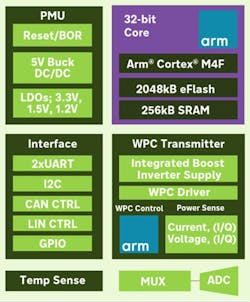
A new Qi wireless in-car charging solution, the result of a collaboration between indie Semiconductor and STMicroelectronics, meets the latest Wireless Power Consortium (WPC) specifications, which call for protection by a secure element. The reference design pairs indie Semi's iND87200 wireless-charging IC with ST's STSAFE-V100-Qi to create a Qi charger that complies not only with the latest WPC specification, but also Common Criteria EAL4, to assure protection of charging devices at up to 15 W.
Special capabilities of indie’s iND87200 wireless-charging IC include an integrated boost converter to maximize charge area and maintain consistent charging power up to 15 W. In addition, integrated advanced power-sensing circuitry monitors system impedance and phase in real-time, as well as the typical voltage and current sensing.
With such an advanced feature, system designers can optimize tuning and algorithms to enable more intelligent features, e.g., adaptive foreign object detection, not otherwise possible in less integrated implementations. The iND87200 also simplifies WPC Qi compliance.
ST's STSAFE-V100-Qi also supports secure boot, secure storage, and secure software update. This extra safeguarding strengthens protection against risks such as remote tampering, counterfeiting, and copying. Designed with secure software updates, the IC ensures a high level of security for the life of the vehicle.
The STSAFE-V100-Qi is sampling now to lead customers and will enter full production in Q4 2023. For more information, go here and here.
650-V Quad-Packed MOSFETs Support Energy-Efficient Fast EV Charging
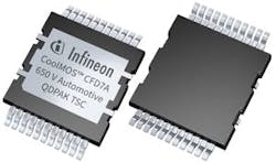
Infineon Technologies added a QDPAK TSC (top-side cooled) package option to its 650-V CoolMOS CFD7A portfolio, intended to support efficient energy utilization in onboard chargers and DC-DC converters. This package family provides thermal capabilities equivalent to the well-known TO-247 THD devices, but with improved electrical performance. In turn, it helps reduce charging times and vehicle weight in onboard charger (OBC) designs, increasing design flexibility and lowering the total cost of ownership of the vehicle.
The 650-V CoolMOS CFD7A offers several important features for reliable operation in high-voltage applications. Thanks to its reduced parasitic source inductance, the device can minimize electromagnetic interference (EMI), ensuring clear signals and consistent performance. The Kelvin source pin also improves precision for current sensing, even in challenging conditions.
With a creepage distance suitable for high-voltage applications, as well as high-current capability and high power dissipation (Ptot) of up to 694 W at 25°C, it’s a versatile and powerful device for a wide range of high-voltage applications.
New system designs using the 650-V CoolMOS CFD7A in QDPAK TSC will be able to maximize PCB space, doubling power density and enhancing thermal management via substrate thermal decoupling. The power switch reduces thermal resistance by up to 35%, providing high power dissipation that outperforms standard cooling solutions.
The QDPAK TSC package has been registered as a JEDEC standard for high-power applications, helping to establish a broad adoption of TSC in new designs with one standard package design and footprint. To further to accelerate this transition, Infineon will also release additional automotive-qualified devices in QDPAK TSC for onboard chargers and DC-DC converters in 2024, such as 750- and 1200-V CoolSiC devices.
The 650 V CoolMOS CFD7A is available in QDPAK package with two versions, top-side cooled (TSC) and bottom-side cooled (BSC). Both variants can be ordered now.
N-Channel Common-Drain MOSFET Supports Bidirectional Power for USB Apps

A new 30-V N-channel common-drain MOSFET, the SSM10N961L from Toshiba Electronics, offers low-loss operation and is intended for use within devices that have USB interfaces and to protect battery packs in mobile applications.
The SSM10N961L combines two N-channels in a common drain configuration that allows for bidirectional operation. The source-source breakdown voltage (V(BR)SSS) is 30 V, which is suitable for higher-voltage applications like laptops and tablets. To reduce losses in all applications, the source-source on-resistance (RSS(ON)) is typically 9.9 mΩ.
The device simplifies design that supports higher power levels and the ability to swap the power supply and receiving side, which was made possible by the USB Power Delivery (USB PD) standard. This includes load switching for power lines of USB charging devices and the protection of Li-ion battery packs for battery-powered appliances.
The device is housed in a small thin package (TCSPAG-341501) measuring just 3.37 × 1.47 x 0.11 mm, allowing for development of high-density solutions. When mounted on a 18-µm, 407-mm2 Cu pad, the current rating of the device is 9.0 A. If the pad size and thickness are increased to 70 µm and 687.5 mm2, the current rating increases to 14.0 A.
By combining the new device with a TCK42xG driver IC, it’s possible to form a load switching circuit with a backflow prevention function or a power multiplexer circuit that can switch operations between make-before-break (MBB) and break-before-make (BBM).
Toshiba also released a power multiplexer circuit as a reference design based on this combination of products. Visit the SSM10N961L product home page for further details.
Compact, Rugged ESD Devices Target Wearables
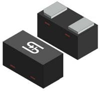
Taiwan Semiconductor’s TESD Series of single-channel ESD clamping diodes offer size and performance specifications optimized for wearable applications. Their unique design features include proprietary bidirectional clamping cells (for ESD protection up to ±30 kV) in an ultra-small DFN0603 package.
Devices in the new TESD Series are offered in versions with 5.0- and 3.3-V (max.) operating voltages and provide protection in compliance with IEC61000-4-2 (ESD) to ±20 kV (air/contact) and IEC61000-4-5 (lightning) to 4.5 A (8/20 µs). A second 3.3-V model in the series increases these specs to ±30 kV and 8.2 A, respectively.
Sam Wang, vice president of TSC Products, said, “Their ultra-small size combined with ultra-low capacitance make these protection devices beneficial in a range of other ESD-sensitive applications, including HDMI, DisplayPort, and high-speed video I/O; USB 3.0 and 3.1; industrial I/O (RS-485); SATA and eSATA; RAID, NAS, and SAN systems.”
With samples available immediately and a lead time of 12 weeks for production quantities, the devices are priced at $0.90 and up. Click here for more information and links to complete product specifications. Design resources include comprehensive datasheets and Spice models for each component in the series.
UK Design Challenge Extends its Quest for Lighter, Cleaner, More Affordable EV Batteries

England's UK Research and Innovation (UKRI) organization extended its Faraday Battery Challenge through 2025 and is inviting new participants to apply for funding to develop and commercialize advanced battery technologies. UKRI, a non-departmental public body sponsored by the Department for Science, Innovation and Technology (DSIT), is investing up to £541 million to further develop a UK battery technology industry aimed at improving:
- Battery lifespan
- Battery range
- Charging rate of batteries
- Reuse, remanufacture, and recycling of batteries
These funds will be used to help underwrite the cost of battery-related feasibility studies, industrial research, and experimental development activities for both academic and commercial organizations.
One group of participants in this next phase is Altair, JLR (Jaguar Land Rover), and battery manufacturer Danecca. They’re collaborating on a project to create a new design process for electric vehicles.
The Challenge's past participants include I-CoBat, a company dedicated to battery cooling technologies, MAT2BAT, a developer of battery module design tools, as well as Nexeon and Echion, which are involved with advanced battery architectures.
A complete list of projects currently funded by the Faraday Challenge is available here. And for more information on the Challenge, visit here.
Read more articles in the This Week in PowerBites Library Series.
About the Author

Lee Goldberg
Contributing Editor
Lee Goldberg is a self-identified “Recovering Engineer,” Maker/Hacker, Green-Tech Maven, Aviator, Gadfly, and Geek Dad. He spent the first 18 years of his career helping design microprocessors, embedded systems, renewable energy applications, and the occasional interplanetary spacecraft. After trading his ‘scope and soldering iron for a keyboard and a second career as a tech journalist, he’s spent the next two decades at several print and online engineering publications.
Lee’s current focus is power electronics, especially the technologies involved with energy efficiency, energy management, and renewable energy. This dovetails with his coverage of sustainable technologies and various environmental and social issues within the engineering community that he began in 1996. Lee also covers 3D printers, open-source hardware, and other Maker/Hacker technologies.
Lee holds a BSEE in Electrical Engineering from Thomas Edison College, and participated in a colloquium on technology, society, and the environment at Goddard College’s Institute for Social Ecology. His book, “Green Electronics/Green Bottom Line - A Commonsense Guide To Environmentally Responsible Engineering and Management,” was published by Newnes Press.
Lee, his wife Catherine, and his daughter Anwyn currently reside in the outskirts of Princeton N.J., where they masquerade as a typical suburban family.
Lee also writes the regular PowerBites series.
Comment About the Article
To join the conversation, and become an exclusive member of Electronic Design, create an account today!

Leaders relevant to this article: