This Week in PowerBites: A Simple Fix to Extend Li-Ion Lifetime Plus SiC, GaN Advances

This article is part of the This Week in PowerBites Library Series.
What you’ll learn:
- A nickel-rich monocrystalline cathode currently under development promises to bring significant improvements to the capacity and lifetime of standard Li-ion batteries.
- Advances in SiC and GaN power devices, and their associated packaging technologies, continues to make EVs more efficient and affordable.
- The trend to re-shore high-tech industries continues with the dedication of a new advanced semiconductor packaging facility in the state of Indiana.
600-V Superjunction MOSFETs for LLC, PSFB Converters and H-4, Solar/ESS Inverters

Alpha and Omega Semiconductor Ltd. introduced two additions to its aMOS5 FRD Super Junction MOSFET series, both rated for 600 V. Both devices address the design challenges posed by today’s mid-high-power switched-mode power supply (SMPS) and solar inverter systems that require extremely high efficiency and density, reduced system costs, and ability to survive harsh conditions.
The AOK095A60FD (TO-247) and AOTF125A60FDL (TO-220F), are 600-V FRD FETs with 95- and 125-mΩ maximum RDS(on), respectively. They offer fast switching and rugged characteristics that suit them for a wide variety of topologies, including single/interleaved/dual-boost/CrCM TP PFCs, LLC, PSFB, and multilevel NPC/ANPC.
These FRD FETs are engineered with strong intrinsic body diodes to handle hard commutation scenarios, when the freewheeling body diode is in reverse recovery due to abnormal operations, such as short-circuit or startup transients. The body diodes of these two FRD FETs have survived high di/dt, under abnormal system conditions, even at elevated junction temperatures of up to 150°C.
In addition, according to AOS, tests have shown that these devices’ turn-off energy (Eoff) are noticeably lower than that of the competition, which contributes to higher efficiency in light- or mid-load conditions.
The AOK095A60FD is immediately available in production quantities with a lead time of 16 weeks. Unit price in 1,000-piece quantities is $3.75. The AOTF125A60FDL is also immediately available in production quantities with a lead time of 16 weeks. Unit price in 1,000-piece quantities is $3.22.
Gate Drivers for 62-mm SiC and IGBT Modules Offer Fast Short-Circuit Protection

A new family of plug-and-play gate drivers is targeted at 62-mm silicon-carbide (SiC) MOSFET and silicon IGBT modules rated up to 1,700 V. The 2SP0230T2x0 dual-channel gate drivers from Power Integrations deploy short-circuit protection in less than 2 µs, protecting compact SiC MOSFETs against damaging overcurrents. The new drivers also include advanced active clamping (AAC) to protect the switches against overvoltage during turn-off, enabling higher DC link operating voltages.
Well-suited for applications such as railway auxiliary converters, offboard EV chargers, and STATic synchronous COMpensator (STATCOM) voltage regulators for the power grid, the 2SP0230T2x0 gate drivers are based on the company’s proven SCALE-2 technology. This results in higher levels of integration, smaller size, more functionality, and enhanced system reliability.
The compact 134- × 62-mm 2SP0230T2x0 provides reinforced isolation at 1,700 V—this is 500 V higher than conventional drivers, which are typically limited to 1,200 V.
SCALE-2 2SP0230T2x0 plug-and-play gate drivers are available for sampling now.
Planar Signal BMS Transformer Increases Reliability/Safety for EV and Energy Storage Systems

According to Bourns, it has developed the industry’s first planar signal BMS transformer. Meeting the need for planar technology that can provide reliable and safe communication in a growing group of high-voltage electric vehicle (EV) and other high-energy storage systems (ESS), the U.S. patented Bourns Model SM91806 Planar Signal BMS Transformer meets basic electric insulation requirements per IEC 60664-1, IEC 61558-1, and IEC 62368-1 standards.
Planar-style signal transformers have been introduced to increase design flexibility and robustness. They’re also known to deliver cost efficiency and reliability advantages over conventional wirewound transformer designs due to their multilayer PCB isolation and full automation.
Offering these benefits and more, Bourns’ new transformer features a working voltage up to 1,000 V DC and superior clearance/creepage distance features, and complies with Overvoltage Category II. It also provides a partial discharge level up to 1,200 V for ESS usage.
For additional product information, go here.
GaN FETs Packaged in CCPAKs Eye Industrial and Renewable-Energy Apps
Nexperia now offers gallium-nitride (GaN) FET devices, featuring next-gen high-voltage GaN HEMT technology, in proprietary copper-clip CCPAK surface-mount packaging that’s suitable for industrial and renewable-energy applications. The GAN039-650NTB, a 33-mΩ (typ.) GaN FET within the CCPAK1212i top-side cooling package, offers improved thermal management and several other advantages for applications such as solar and residential heat pumps. It’s also suited for servo drives, switched-mode power supplies (SMPS), servers, and telecom.
CCPAK surface-mount packaging uses Nexperia’s unique copper-clip package technology to replace internal bond wires. This reduces parasitic losses, optimizes electrical and thermal performance, and improves device reliability. For greater flexibility in designs, the CCPAK GaN FETs come in top- or bottom-cooled configurations to further improve heat dissipation.
The cascode configuration of the GAN039-650NTB enables it to deliver superior switching and on-state performance, with a robust gate offering high margins against noise. This feature also eliminates the requirement for complex gate drivers and control circuitry, instead allowing applications to be conveniently driven using standard silicon MOSFET drivers. In addition, device RDS(on) is reduced to only 33 mΩ (typ.) at 25°C, with a high threshold voltage and low diode forward voltage.
Nexperia began its CCPAK portfolio release with the top-cooled 650-V GAN039-650NTB, and will follow shortly with the bottom-cooled GAN039-650NBB variant.
On-Shoring News: Indiana Breaks Ground for Power-Semi Packaging Assembly Facility

On January 19, NHanced Semiconductors hosted a ribbon-cutting for its NHanced WestGate Facility, a multimillion-dollar advanced package assembly center located in Odon, Indiana. The new facility features two state-of-the art cleanrooms for semiconductor advanced package assembly and test, as well as process development.
The NHanced package assembly line is designed as part of WestGate One—a multi-company complex that will be the first semiconductor foundry in the U.S. built specifically for advanced package manufacturing. NHanced will be the anchor tenant, along with three other semiconductor companies, at the 10-acre public-private development.
"There will be a mix of defense and commercial products," said NHanced president Bob Patti. "Offshore facilities typically only do high-volume manufacturing, and this is not a high-volume manufacturing facility, so the marginally higher cost of our services is really not a factor."
Patti explained that the largest factors influencing the facility’s location include its proximity to the planned NHanced foundries in Westgate and Bloomington, Indiana, economic incentives, and the presence of numerous educational institutions.
"These institutions are actively producing engineers, particularly those with a strong focus on packaging technologies,” said Patti. “These engineers are crucial for the facility as it ensures a local talent pool well-versed in packaging technologies. This not only facilitates the recruitment of skilled professionals, but also fosters collaboration with educational institutions for ongoing advancements and innovation in the field.”
NHanced, headquartered in Illinois, is a pure-play advanced packaging foundry specializing in leading-edge BEoL semiconductor technologies, including chiplets, 3D-ICs, silicon interposers, 2.5D, additive silicon manufacturing, photonics, microfluidics, and other innovative technologies.
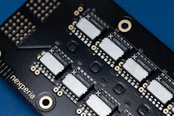
LCD Bias Power ICs Extend Battery, Display Lifetime in Smartphones and VR Headsets

A new series of space-saving, high-efficiency, dual-output LCD bias power supplies was recently unveiled by Nexperia. These devices are designed to extend the lifetime of thin-film-transistor liquid-crystal-display (TFT-LCD) panels used in an array of applications, including smartphones, tablets, virtual-reality (VR) headsets, and LCD modules.
The NEX10000 is an 80-mA dual-output LCD bias power supply, while the NEX10001 can deliver up to 220 mA of output current. Both devices feature I²C programmable asymmetric voltage outputs. The devices are internally compensated and require only a single inductor for both outputs, allowing for a small bill of materials and PCB area.
To address low-power considerations in TFT-LCD applications that require longer battery life, the NEX10000/1 integrate a boost converter. Depending on the load current, they can operate either in continuous conduction mode (CCM) or pulse frequency modulation (PFM) mode to provide the highest level of efficiency for operation on single-cell Li-ion, Ni-Li, and Li-polymer batteries. Both devices have an input voltage range of 2.7 to 5 V and offer excellent line and load transient responses.
To minimize the amount of board area required in space-constrained applications, the NEX10000/1 come in a wafer-level chip-scale package (WLCSP) with 15 bumps and a 1.16- × 1.96- × 0.62-mm form factor, which is even smaller than standard wafer-level packages.
Learn more about Nexperia’s new power ICs here.
All-SiC Power Modules Enable Smaller Fast-Charging Platforms with Bidirectional Charging

Nine new EliteSiC power integrated modules (PIMs) from onsemi support bidirectional-charging capabilities for DC ultra-fast electric-vehicle (EV) chargers, and bidirectional charging applications for EVs and larger energy storage systems (ESS). The silicon-carbide-based solutions offer high efficiency and simpler cooling mechanisms that can reduce size by up to 40% and weight by up to 52% compared to traditional silicon-based IGBT solutions.
Several important design and manufacturing features of these modules are intended to maximize performance and reliability:
- To deliver the best possible consistency and reliability, each module is fabricated with power ICs from the same wafer.
- The modules support key topologies such as multi-level T-type neutral point clamp (TNPC) andhalf-bridge and full-bridge topologies for applications requiring 25 to 100 kW.
- Industry-standard F1 and F2 packages with the option of pre-applied thermal interface material (TIM) and press fit pins.
Additional information can be found at the following links:
- EliteSiC Power Integrated Modules
- Read the latest white paper: Review of Power Converter Topologies for DC Fast Charging and Ultra-Fast Charging Applications
- Simulate with Elite Power Simulator and Self-Service PLECS Model Generator
Synchronous Buck Regulators Equipped with Fast COT Architecture to Handle DC-DC POL Apps
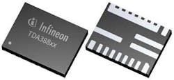
Infineon's new TDA388xx series of synchronous buck regulators addresses the growing need for compact, highly efficient power-conversion solutions, especially for server, AI, datacom, telecom, and storage applications. The 12- and 20-A devices operate over a wide input voltage range from 4.0 to 16 V and utilize a fast constant on-time (COT) control scheme. This approach not only delivers high efficiency, but also rapid transient response, as well as minimizing passive component count that leads to reduced board space requirements.
The TDA388xx family (TDA38812, TDA38813, TDA38825, and TDA38826) employs a unique internal compensation technique that improves ease of use and reduces the need for external components. It also offers selectable switching frequencies and a soft-start functionality, as well as a programmable current limit. All regulators in the series support fixed-frequency continuous conduction mode (FCCM) and discontinuous conduction mode (DCM). In addition, voltage tracking is enabled through an external reference input.
The key to the TDA388xx series is its built-in protection features to ensure system safety during fault conditions. These include pre-bias startup and thermally compensated current limiting. Overvoltage protection (OVP) and undervoltage protection (UVP) are also built in. Furthermore, a thermal shutdown is included for added safety. The series is housed in a ROHS-compliant QFN-21 package. It operates effectively over a temperature range of −40 to 125°C.
The TDA388xx family, which comes in a standard QFN-21 (3 × 4 mm) package, can be ordered now. More information is available here.
Roll-Your-Own Printed Stator Motors: Cloud Design Platform for Lighter, Smaller Custom PMSMs
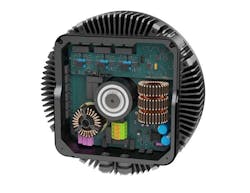
U.S. electric motor design and software company ECM PCB Stator Tech announced the public release of its PrintStator Motor CAD software-as-a-service (SaaS) platform, intended to transform the way electric motors are devised and manufactured. As a SaaS offering, the Motor CAD platform enables companies with manufacturing capacity to advance designs immediately to production.
ECM’s PCB stators replace the bulky copper windings in traditional motors with an ultra-thin disc. PCB stator motors designed via PrintStator are up to 70% lighter than conventional options, while achieving efficiencies in the mid-90s and requiring just 20% of the raw materials.
From the platform's cloud-based interface, PrintStator users can dial-in precise performance and dimensional specs to create custom electric-motor solutions for multiple verticals: consumer electronics, HVAC, e-mobility, medical, robotics, aerospace, and more. This enables PrintStator users without manufacturing capability to use nearly any industry-compliant PCB manufacturer as a source for rapid production of their perfect-fit electric motors.
You can explore the PrintStator SaaS platform's capabilities via this video: “How Does a PCB Stator Work?”, or by visiting ECM’s Design Your Own page.
High-Voltage, Automotive-Compliant, Hall-Effect Latches Improve Resistance to Physical Stress
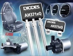
The AH371xQ series of high-voltage Hall-effect latches developed by Diodes Inc. feature a proprietary Hall plate design that boosts performance. Such devices are used for brushless DC (BLDC) motor control, valve operation, linear and incremental rotary encoders, and position-sensing functions.
As a result, the automotive-compliant AH371xQ series can support numerous in-vehicle comfort and engine management applications—window power-lift and sunroof movement, tailgate opening/closing mechanisms, seat adjustment motors, cooling fans, water/oil pumps, and speed measurement.
The latches have an operating voltage range from 3 to 27 V, with 40-V load dump protection. Their chopper-stabilized design mitigates the effects of thermal variation and provides enhanced stray field immunity. Power-on time is typically 13 µs.
Six sensitivity options are available, ranging from 25 to 140 gauss, all with tight operating windows and low switch point temperature coefficients. These options give engineers scope for different magnetic operating (BOP) and magnetic release (BRP), enabling designers to find the best fit between the sensing distance and the magnets used for their application. Open-drain outputs lead to greater external pull-up flexibility when it comes to voltages that are higher or lower than the supply voltage.
The latches in the AH371xQ series have an 8-kV human-body-model (HBM) electrostatic-discharge (ESD) rating. Protection features include reverse blocking diode, overcurrent protection, and overvoltage clamp.
All devices are AEC-Q100 Grade 0 qualified, manufactured in IATF 16949 certified facilities, and support PPAP documentation. The family comes in SOT23 (Type S), SC59, and SIP-3 (Bulk Pack) packages, while the AH3712Q is also available in U-DFN2020-6 (SWP) packages. Pricing is $0.32 in 1,000-piece quantities. These, along with the full portfolio of Hall-effect sensors, are included in the Hall-effect sensor part selector.
More Range for EV Batteries on the Horizon with Monocrystalline Li-Ion Batteries

A seemingly simple shift in lithium-ion battery manufacturing could pay big dividends, improving an electric vehicle’s (EV) ability to store more energy per charge and withstand more charging cycles, according to new research led by the U.S. Department of Energy’s Pacific Northwest National Laboratory (PNNL). The potential breakthrough is the Labs' new nickel-rich, single-crystal battery technology that’s on track for rapid deployment.
An EV’s mileage depends on the deliverable energy from each of the constituent cells of its battery pack. For lithium-ion cells—which dominate the EV battery market—both the cell-level energy capacity and the cell cost are bottlenecked by the positive electrode, or cathode.
Now that bottleneck might be opening up, thanks to an innovative, cost-effective approach for synthesizing single-crystal, high-energy, nickel-rich cathodes that was recently published in Energy Storage Materials.
The Nickel-Rich Battery Vision
Cathodes for conventional EV batteries use a cocktail of metal oxides—lithium-nickel manganese cobalt oxides (LiNi1/3Mn1/3Co1/3O2), abbreviated NMC. When more nickel is incorporated into a cathode, it greatly increases the battery’s ability to store energy, and thus, the range of the EV.
However, high-nickel NMC cathodes formed using the standard method are agglomerated into polycrystal structures that are rough and lumpy. At higher levels of Ni concentration, the bulbous polycrystal fissures are prone to splitting apart, causing material failure and thus making the nickel-rich cathodes susceptible to cracking. In addition, they begin to produce gases and decay faster than cathodes with less nickel.
Battery developers have known for some time that these problems can be cured by converting that lumpy, polycrystal NMC into a smooth, single-crystal form by eliminating the problematic boundaries between the crystals—but it has proven to be a difficult task. Until recently, most researchers tried to form monocrystalline cathode structures by mixing a metal hydroxide precursor with lithium salt, directly mixing and using a multiple-step heating process which was only partly successful.
PNNL’s Solution
Led by PNNL battery experts, and in collaboration with Albemarle Corp., the research team solved these issues by introducing a pre-heating step that changes the structure and chemical properties of the transition metal hydroxide. When the pre-heated transition metal hydroxide reacts with lithium salt to form the cathode, it creates a uniform single-crystal NMC structure that looks smooth, even under magnification.
The first prototype battery equipped with the scaled single crystals was stable, even after 1,000 charge and discharge cycles. When the researchers looked at the microscopic structure of the crystals after 1,000 cycles, they found no defects and a perfectly aligned electronic structure.
Rapid Deployment of EV Battery Technology
In the research phase, set to begin in early 2024, PNNL, teaming up with industry and university partners, will work to realize commercial-scale synthesis and testing with an eye toward production.
To accomplish this so quickly, they will use conventional manufacturing equipment and techniques that have been industrially adapted to include PNNL’s scale-up approach (as well as a few other innovations that further reduce costs and waste generation).
Read more articles in the This Week in PowerBites Library Series.
About the Author

Lee Goldberg
Contributing Editor
Lee Goldberg is a self-identified “Recovering Engineer,” Maker/Hacker, Green-Tech Maven, Aviator, Gadfly, and Geek Dad. He spent the first 18 years of his career helping design microprocessors, embedded systems, renewable energy applications, and the occasional interplanetary spacecraft. After trading his ‘scope and soldering iron for a keyboard and a second career as a tech journalist, he’s spent the next two decades at several print and online engineering publications.
Lee’s current focus is power electronics, especially the technologies involved with energy efficiency, energy management, and renewable energy. This dovetails with his coverage of sustainable technologies and various environmental and social issues within the engineering community that he began in 1996. Lee also covers 3D printers, open-source hardware, and other Maker/Hacker technologies.
Lee holds a BSEE in Electrical Engineering from Thomas Edison College, and participated in a colloquium on technology, society, and the environment at Goddard College’s Institute for Social Ecology. His book, “Green Electronics/Green Bottom Line - A Commonsense Guide To Environmentally Responsible Engineering and Management,” was published by Newnes Press.
Lee, his wife Catherine, and his daughter Anwyn currently reside in the outskirts of Princeton N.J., where they masquerade as a typical suburban family.
Lee also writes the regular PowerBites series.
Comment About the Article
To join the conversation, and become an exclusive member of Electronic Design, create an account today!

Leaders relevant to this article: