

Various digital circuits require push-pull power drivers, particularly for gate and line driver applications. Many special-purpose devices are available for these issues, but they are typically expensive and single-sourced, with a short product lifecycle that forces a costly redesign when they are discontinued. Fortunately, the ubiquitous LM555 timer (non-CMOS versions) can serve as a very inexpensive and capable driver.
With its powerful totem-pole output and a 4.5- to 16-V supply range, the LM555 can be used as either a buffer or an inverter. If more than one driver is required, designers can use the dual LM556 to reduce cost and footprint. The rare 558, a quad version, can also be applied as a quad inverting driver.
To implement a buffer function, configure the timer’s reset line (pin 4) as the input (Fig. 1). This provides a transition level of 0.5 to 1 V, allowing the device to be driven directly by standard 5-, 3.3-, and even 1.8-V logic regardless of the VCC level. Alternatively, the trigger line (pin 2) may serve as an active-low enable line, although this line does not have the same compatibility as the reset pin in terms of levels.
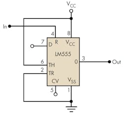
1. By using the LM555’s reset pin as the input, the timer can serve as a buffer circuit driven by standard logic levels from 1.8 to 5 V.
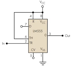
In the inverting configuration, the trigger line is used as the input, with a transition threshold of 0.334 × VCC (Fig. 2). Additionally, the reset line could be used as an active-high enable line with the same transition levels, including the 1.8-V logic level, as stated above.
With its 200-mA sink/source capability, an LM555 powered by 12 or 15 V can drive most MOSFET/IGBT gates at frequencies exceeding 250 kHz without clamping diodes on the gate, minimizing cost. When driving gates, you should place a 5- or 10-Ω resistor in series with the output to minimize ringing and transient currents. In addition, the circuit should include a ceramic or tantalum bypass capacitor or at least 1 µF to provide the surge currents required.
Both of the circuits also provide an additional open-collector output on the discharge pin (pin 7) that could be set to any voltage level, up to 18 V. You can let the control voltage pin (pin 5) float, or you could use it to change the internal comparator threshold levels.

About the Author
Comment About the Article
To join the conversation, and become an exclusive member of Electronic Design, create an account today!

Leaders relevant to this article: