Hex Buffer, MOSFETs Build A High-Power, Lossless, Virtual Ground

This file type includes high resolution graphics and schematics.
A virtual ground is useful whenever you need to create a bipolar supply but the dc source is unipolar, as is often the case with battery-operated equipment. Sometimes, the solution is as easy as using a high-ohm resistive divider to provide a mid-supply potential. But if the ground impedance needs to be lower, the simple approach can be enhanced by using a buffer amplifier.
Related Articles
- Understanding Amplifier Operating "Classes"
- Reduce EMI In Your Class D Amplifiers
- Essential Steps For Making High-Quality Electrical Measurements
When the ground created this way sees high imbalance currents, though, things become more complicated. The buffer not only needs to be a power buffer, it will also have to dissipate the result of any imbalance. This is wasteful, and it may even require bulky, inconvenient heatsinks.
This circuit addresses these issues simply, cheaply, and effectively (see the figure). It retains the resistive divider plus buffer configuration, but with a big difference. The buffer is now a self-oscillating Class D amplifier, capable of providing many amperes of ground current and of “recycling” any imbalance back to the supply. The circuit is compact and efficient, while providing a stiff, accurate, and powerful ground.
The oscillator is built around a simple CD4069 CMOS hex buffer. Most of its inverters act as gate drivers for the power MOSFETs. Inverter U1 provides the non-inverting input of the amplifier, as the inverting input is implicit and is represented by the CD4069’s mid-supply potential. Capacitor C3 provides positive feedback and allows the circuit to self-oscillate.
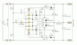
The entire control circuit has a floating supply referenced to the output. Diodes D3 to D6 and resistor pair R6/R7 generate this supply from the dc input. R2 and R3 create the virtual ground potential. In this example, they are equal, as will generally be the case, but asymmetrical supplies also can be created.
For greater accuracy, a trim potentiometer can be added to the midpoint of R2/R3. With the values shown, the pulse-width modulation (PWM) frequency is approximately 45 kHz, which can be modified by changing C3.
The power MOSFETs and inductor must be sized according to the expected output current. If a very clean ground is required, an additional LC filter can be used after L1 and C6/C7 to clean up the remaining switching residues.
Louis Vlemincq works as a design engineer in Physcial Layer Engineering at Belgacom, Evere, Belgium. He can be reached at [email protected].
This file type includes high resolution graphics and schematics.
About the Author
Louis Vlemincq
Design Engineering Director
Louis Vlemincq works as a design engineer in Physcial Layer Engineering at Belgacom, Evere, Belgium. He can be reached at [email protected].
Comment About the Article
To join the conversation, and become an exclusive member of Electronic Design, create an account today!

Leaders relevant to this article: