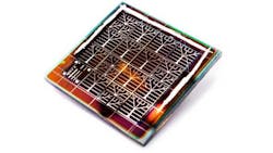
A solar cell based on copper zinc tin selenide (CZTSe) achieves 9.7% efficiency, according to its joint development team of Solliance, the European research consortium working on thin-film photovoltaic (PV) solar energy, and Imomec, a laboratory associated with Belgian research center Imec (see the figure).
Similar to CZTS (copper, zinc, tin, sulphur), CZTSe is viewed as a possible alternative solar-cell absorber in thin-film solar cells. However, both are unlike CIGS (copper, indium, gallium, selenide), in that CZTS and CZTSe don’t suffer from abundancy issues regarding the availability of manufacturing material.
Another key is that CZTS comes in at 1.5-1.6 eV and CZTSe at 0.9 eV. Thus, their bandgaps (an energy range in a solid where no electron states can exist) make a combined material system suitable for a multi-junction, thin-film solar cell that rivals CIGS cell efficiency.
Industry experts consider this development as a crucial step toward providing the solar-power industry with a sustainable alternative to today’s CIGS-based, high-efficiency, thin-film solar cells. Accordingly, Imomec, Imec, and Solliance established a development roadmap aimed at further improving the layers and cell structures of CZTSe and CZTS absorbers. The goal is to create a multi-junction CZTS/CZTSe solar cell that achieves 20% efficiency.
Imec/Imomec fabricated the CZTSe layers by sputtering metal layers on a molybdenum-on-glass substrate and then annealing them in an H2Se-containing atmosphere. The resultant polycrystalline absorber layers were 1-µm thick, with a typical grain size of about 1 µm.
The samples were subsequently processed at Helmholtz Zentrum Berlin into solar cells using a standard process flow for thin-film solar cells. Imec then finished the samples with a metal grid and anti-reflective coating.
The highest efficiency obtained on a 1- by 1-cm2 cell was 9.7%, with a maximum short-circuit current of 38.9 mA/cm2, an open-circuit voltage of 0.41 V, and a fill factor of 61%.
Environmentally Safe OPV Cells
In an earlier development, Solliance believes it achieved the first inkjet printing process for manufacturing environmentally friendly OPV (organic photovoltaic) cells that deliver benchmark efficiency. Claimed to be compatible with existing manufacturing technology, the process replaces toxic chlorinated solvents with benign alternatives.
OPVs promise cheaper solar cells that can be flexible, lightweight, semi-transparent and easily integrated into construction materials. Until now, however, OPV production processes relied on coating techniques and chlorinated solvents. These highly toxic solvents, which could cause river contamination and killing of wildlife, are banned substances for industrial manufacturing applications.
So far, OPVs have been limited to lab-scale production. With Solliance new process, though, the photo-active layers can be inkjet-printed on a prodcution basis without using poisonous chlorinates. The breakthrough, achieved in collaboration with French OPV manufacturer DisaSolar, falls within the framework of the European project X10D.
The basis of the process is a blend of low-toxicity solvents. The solvents provide a stable base that achieves the right level of viscosity and surface energy of the inks, allowing for printing of OPVs. The final OPV cells deliver performances comparable to the spin-coated counterparts from standard chlorinated solvents—approximately 3% efficiency for a P3HT:PCBM photoactive layer system.
About the Author
Paul Whytock
Voice Your Opinion!
To join the conversation, and become an exclusive member of Electronic Design, create an account today!

Leaders relevant to this article:
