Simple Addition Permits Voltage Control Of DC-DC Converter's Output

This file type includes high resolution graphics and schematics.
In a standard dc-dc converter, a resistor divider typically defines a fixed output voltage. However, applications like programmable output voltage power supplies and motor control circuits require dynamic control of the dc-dc converter’s output voltage. The circuit described here allows control of the converter’s output voltage, VOut, with a control voltage, VC.
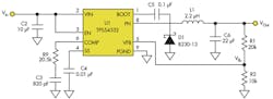
In a conventional dc-dc buck converter, VOut is:

so VOut is fixed by the values of R1 and R2 (Fig. 1).
The added circuitry in Figure 2 enables users to control the same dc-dc converter’s output voltage using VC.
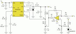
In this case, R2 is not connected to the ground but, rather, to Vr. Equation 1 then becomes:

Since R1 = 20 kΩ and R2 = 10 kΩ, Equation 2 can be simplified to:
VOut – Vr = 3(Vfb – Vr)(3)
or:
VOut = 3 Vfb – 2 Vr(4)
R3 and R4 have the same value, 10 kΩ, so amplifier U2’s output voltage is:
Vr = 2 VRef – VC(5)
where VRef is the reference voltage generated by U3 after resistor divider R7/R8.
Combining Equation 4 and Equation 5:
VOut = 3 Vfb – 4 VRef + 2 VC(6)
To simplify Equation 6, choose components that make:
3 Vfb = 4 VRef(7)
Then Equation 6 becomes:
VOut = 2 VC (8)
The internal voltage reference of U1 is 0.8 V. By choosing R7 = 10 kΩ and R8 = 3.16 kΩ, VRef = 0.6 V, satisfying Equation 7. Finally, C1 lowers U2’s output impedance at high frequencies, maintaining the stability of U1’s feedback loop.
The added circuitry allows users to control the buck converter’s output voltage, VOut, in the range of 0 to 5 V with a control voltage, VC, in the range of 0 to 2.5 V. Similar circuitry can be designed for use with a boost converter, or any other dc-dc converter, as long as its feedback voltage pin is accessible.
This file type includes high resolution graphics and schematics.
>> Electronic Design Resources
.. >> Library: Article Series
.. .. >> Series: Ideas for Design
.. .. .. >> Ideas for Design Volume 2
About the Author
Eugene Palatnik
President
Eugene Palatnik is an electrical engineer and president of ITEC Engineering LLC. He is active in the design of electronics for medical, scientific, and industrial applications.
Comment About the Article
To join the conversation, and become an exclusive member of Electronic Design, create an account today!

Leaders relevant to this article: