Flexible, Multi-Output Supplies Conquer Complex SoC Power Challenges
Download this article in PDF format
Over the last few years, system-on-chip (SoC) devices incorporating multicore processors have been appearing in a wide variety of consumer and industrial products. Samsung’s Galaxy 8 S8 smartphone is powered by Qualcomm’s Snapdragon eight-core 3.2-GHz processor; Apple’s latest A9 SoC, used in the iPhone 6S, includes the company’s own ARMv8-A dual-core CPU plus a six-core graphics processing unit (GPU).
Integrated circuits based around field-programmable gate arrays (FPGAs) are also adding multicore processing power and other functional blocks to form SoCs. For example, in addition to its programmable logic, digital-signal-processor (DSP) block, and an array of peripheral functions, the Xilinx Zynq-7000 SoC includes a single- or dual-core ARM Cortex-A9 processor. These FPGA-based devices are used for digital signal processing, software-defined radio, cellphone base stations, medical imaging, computer vision, cryptography, speech recognition, and many other applications.
Supplying power to these devices, with their CPUs, GPUs, and DSPs, is no easy task for the power system designer: SoCs require very high current and very fast response time. They have multiple different voltage rails that must be powered on and off in a precisely controlled sequence.
Small size is a must-have, too. From smartphones to server line cards, the demand is to fit more features into a smaller form factor. This places a premium on reducing the number of components, maximizing conversion efficiency, and minimizing overall power consumption.
Repurposing the Multiphase Converter Topology
The SoC power supply must generate multiple low-voltage outputs with high efficiency and fast transient response. These goals require a combination of linear and switching technologies, and designers are finding new uses for old power-converter architectures.
The multiphase buck converter is widely used in applications that require high output current and fast transient response because it overcomes the conventional single-phase buck converter’s fundamental limitation—the reduction in conversion efficiency as switching frequency increases.
Boosting the switching frequency has many advantages: it reduces the output ripple; increases dynamic response; and allows the use of smaller inductors and capacitors. The drawback is escalating switching losses that in turn reduce efficiency.
Combining multiple interleaved converters with phase-shifted switching effectively multiplies the fundamental frequency by the number of phases, with corresponding improvements in performance and reductions in component size. At the same time, each individual converter has lower switching losses, hence higher efficiency.
Traditional multiphase architectures don’t allow the designer to set the parameters of each individual single-phase block, but the LP8758 multiphase converter from Texas Instruments removes that restriction. In addition to the normal four-phase operation with the outputs combined, each of the LP8758’s converters can act as an independent device.
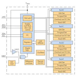
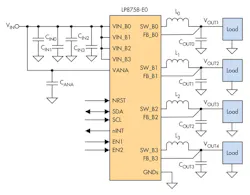
The LP8758 combines four buck-regulator output stages with a common digital logic block, voltage reference, and thermal protection circuitry (Fig. 1). In addition to acting as a traditional multiphase converter, the device can generate four separate 0.5- to 3.36-V regulated voltage outputs from a 2.5- to 5.5-V input. In this configuration (Fig. 2), the LP8758 outputs default voltages of 1, 2.5, 1.2, and 1.8 V (Buck0-Buck3). An external microcontroller can change the individual output voltages and current limits via an I2C interface.
The microcontroller also is able to sequence the startup and shutdown operations of the regulators, making it ideal for an SoC or similar application. Sequencing can be accomplished either via the enable pins EN1 or EN2 or through the I2C interface. Delays from 1 to 15 ms are possible.
Switching regulators are inherently noisy. To reduce electromagnetic interference (EMI), the LP8758 features a selectable spread-spectrum mode, controlled via I2C. In this mode, the switching frequency varies randomly by ±5% (depending on the selected switching frequency) about the center frequency. This reduces the emissions radiated by the converter and associated passive components and PCB traces. Furthermore, it reduces design size by eliminating the need for output filters, ferrite beads, or chokes.
Designing a Compact Solution for an FPGA SoC
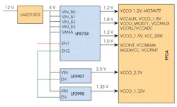
Figure 3 shows the LP8758 as part of a power solution for the Xilinx Zynq-7015 SoC, a member of the Zynq-7000 family. The Zynq-7015 power-on sequence recommends that the processing-system (PS) power rails—VCCPINT (1.0 V), VCCPAUX (1.8 V), and VCCPLL (1.8 V)—be powered up before the input/output (I/O) power. This sequence achieves the minimum current draw and ensures that the I/O ports are in the high-impedance (tri-state) condition at power-on.
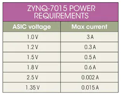
For the Zynq-7015, the LP8758 output voltages are set to 1.0, 1.2, 1.5, and 1.8 V. The output-voltage slew rate at startup is set to 10 mV/µs, and the current limits are set based on the requirements of the Zynq-7015 (see table below).
Reducing Power Consumption with Dynamic Voltage Scaling
The power-supply microcontroller can vary the LP8758 output voltages in response to inputs from the Zynq-7015. This reduces average power consumption, a technique known as dynamic voltage scaling (DVS). DVS allows the system designer to trade off performance for power consumption. Reducing the voltage slows the SoC, but it also reduces power consumption. Lower power consumption increases the battery runtime in portable devices; the SoC also generates less heat, which reduces the load on the cooling system and potentially leads to longer product life.
Other power devices used in this design include:
• The LMZ31503, a member of TI’s SIMPLE SWITCHER power-module family, provides the first-stage power conversion from 12 V to 5 V. This device integrates a dc-dc converter, power MOSFETs, a shielded inductor, and passives into a single low-profile QFN package. It can require as few as three external components; the high level of integration also simplifies the design by eliminating the loop compensation and magnetics selection steps. For this application, the LMZ31503 provides a 5-V output at up to 3 A of load current.
• Two linear low-dropout (LDO) regulators deliver power to the Zynq-7000’s HR and HP I/O banks. Although linear regulators are typically less efficient than switching designs, these are both low-current rails—linear regulators reduce the layout size and minimize the BOM. Both devices have logic-level enable pins and fit well into this sequenced application.
—The LP3990 LDO regulator supplies 1.35-V power. This device is suitable for a wide variety of portable and battery-powered systems. Devices in the family can supply up to 150 mA with outputs ranging from 0.8 to 3.3V.
—The LP5907 supplies 2.5 V at up to 250 mA. Among the features of this device are low noise, high PSRR, low quiescent current, and excellent line or load transient response. The LP5907 doesn’t require a noise bypass capacitor, and the output capacitor can be situated remotely for greater layout flexibility.
Power-Supply Design Guidelines
For best performance in any switching design, it’s important to pay attention to the layout, especially when it involves high switching frequencies and high currents.
Recommended layout guidelines include keeping noise-sensitive traces, such as remote voltage sensing lines, away from high-bandwidth I2C traces, as well as noisy power and ground lines. Route power and grounds on thick layers to avoid IR drops and minimize the trace lengths of both the input capacitors and the output filter inductors and capacitors. Isolate analog inputs from noisy traces and place analog decoupling capacitors as close to the pins as possible.
Correct selection of passive components is also important. For example, the LP8758’s inductors should have a minimum effective inductance overtemperature of 0.22 µH at a bias current of 4 A. For high efficiency, they should have a dc resistance of less than 0.05 Ω over their operating temperature range.
The input requires ceramic capacitors of dielectric types X5R or X7R placed close to the VIN_Bx input pins. These should be at least 10 µF and 6.3 V, although larger values can improve input voltage filtering.
The LP8758 output capacitors smooth out current flow from the inductors to the load, help maintain a steady output voltage during transient changes in load, and reduce the output voltage ripple. These capacitors must therefore have sufficient capacitance and sufficiently low ESR and ESL to perform these functions. Minimum effective output capacitance is 10 μF per phase at the output-voltage dc bias voltage, including tolerances over the ambient temperature range.
The input capacitors for the LDO regulators can be ceramic, tantalum, or film, but must be at least 1 µF for good transient performance. In addition, they must be located close to the input pins and connected to a low-noise analog ground. Ceramic output capacitors (X7R or X5R types) from 1 to 10 F are recommended, again with a good GND connection.
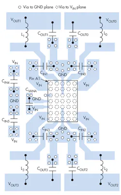
To help, TI has made available a reference design, including design files. For more details about layout, component selection, and thermal management, consult the reference design guide. The design guide includes example layouts for the LP8758 (reproduced in Figure 4) as well as for the LDO regulators.
Other Applications: Server Line-Card Power Supply
Many other applications are space-constrained and require a flexible and compact multi-output power supply: server line cards, for example. These cards perform a variety of functions and contain integrated circuits (ICs) such as serializer/deserializer (SERDES), memory devices, DSPs, and SoCs, all potentially with different voltage, current, and sequencing requirements.
The push toward modular designs, spearheaded by the Open Compute Project (OCP), has also driven new server specifications and new smaller form factors for pluggable server line cards. The OCP is a collaborative effort that’s working to develop a highly efficient scalable computing architecture with shared intellectual property (IP). Originally begun by Facebook, members now include familiar names—Google, IBM, Intel, Microsoft, Lenovo, Ericsson—as well as some surprising ones—Goldman Sachs and Fidelity Investments.
The LP8758 is useful in this application, too. TI has produced a compact multi-rail line-card reference design that has an input voltage of 3.3 V and outputs of 1.0, 1.2, 1.8, and 2.5 V. The reference design features power-supply sequencing, DVS, and a host microcontroller to communicate with the load device.
Conclusion
The drive toward increasing functionality in smaller packages has led to the integration of diverse feature sets into SoC devices. These devices have complex power requirements with multiple low-voltage rails that must be sequenced in a defined order.
In response, designers have combined switching and linear power-conversion techniques and digital control to develop flexible, multi-output power architectures that can accommodate variable sequences and voltage combinations. As such, the configurable LP8758 multiphase converter is well-suited for this application.
About the Author
Paul Pickering
Paul Pickering has over 35 years of engineering and marketing experience, including stints in automotive electronics, precision analog, power semiconductors, flight simulation and robotics. Originally from the North-East of England, he has lived and worked in Europe, the US, and Japan. He has a B.Sc. (Hons) in Physics & Electronics from Royal Holloway College, University of London, and has done graduate work at Tulsa University. In his spare time, he plays and teaches the guitar in the Phoenix, Ariz. area
Voice Your Opinion!
To join the conversation, and become an exclusive member of Electronic Design, create an account today!

Leaders relevant to this article:
