Take a Practical Path Toward High-Performance Power Conversion
This file type includes high-resolution graphics and schematics when applicable.
In power conversion, fast switching combined with high efficiency enables small size, low weight, and lower system cost. To achieve this, we need to consider the choice of topology, power switch, and magnetic materials. Soft-switching techniques, coupled with novel gallium-nitride (GaN) power ICs and updated high-frequency-optimized transformers and inductors, offer a way to boost the efficiency and power density in ac-dc converters.
Traditional “hard-switching” topologies like quasi-resonant-flyback (QRF) or forward converters have loss in snubber networks and within the switching devices that cannot be eliminated. The soft-switching or zero-voltage-switching (ZVS) technique used in active-clamp-flyback (ACF) and LLC converters is a modern, elegant approach to recycling energy within the topology and minimizing loss. Reducing loss, and minimizing transition times and “deadtimes” per switching cycle, allows for faster switching frequency, and in turn reduces the size and cost of magnetic materials.
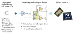
For power switching, GaN is a new “wideband gap” semiconductor material with 100X faster switching and 20X improved “RxQG” performance than silicon (Si). Early implementations such as depletion mode (dMode), cascoding, and discrete approaches were vulnerable to voltage transients (noise) and required precise voltage control to extract GaN’s potential. This led to large, complex circuits that restricted the switching speed of the application.
To help solve this problem, Navitas Semiconductor developed the AllGaN process design kit1, which uses GaN’s lateral structure to enable the monolithic integration of power FETs, drivers, and logic into a single IC (Fig. 1). Integration is key to minimize delays and eliminate parasitic inductances that restricted the switching speed of Si and earlier discrete GaN circuits. With propagation delays down to 5 ns, and dV/dt up to 200 V/ns, traditional 65- to 100-kHz converter designs can be accelerated to 1 MHz and beyond.
Adding Flexibility
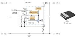
Discrete gate-drive circuits are complex, with high component count and a long design cycle. The digital input of GaN Power ICs (Fig. 2) creates flexibility in design, with options for the power switches to be placed on the main board or on a daughtercard, close to or far from the control IC. Precise internal voltage regulation and no parasitic path to the GaN FET gate ultimately leads to a simple, minimal-component-count, rugged solution. In addition, features like programmable dV/dt and UVLO help maximize flexibility.
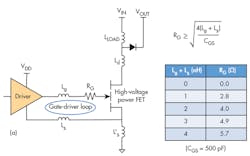
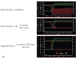
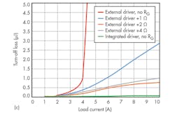
To better understand the integrated gate drive, let’s study2 the effects of a simple gate-drive “damping” resistor (RG), typically used with traditional driver ICs to control the voltage (reduce oscillation) and protect the vulnerable discrete FET gate. In the progression of Figs. 3a to 3c, we see that with external drivers, just 1 to 2 nH of gate loop inductance can cause unintended turn-on. While gate resistors reduce the voltage spikes, they create additional losses. Thus, the system becomes limited in terms of switching frequency. Only by integrating the gate drive onto the same die as the FET (eliminating gate resistance and impedance) is it possible to achieve stability and high efficiency.
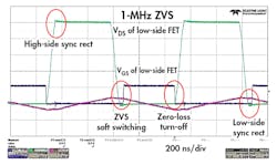
Moving from the study of a single switch to a half-bridge implementation, we can see that the switching waveforms—even at a frequency of 1 MHz—exhibit a true “text book” appearance, with very clean rising and falling edges and no ringing (Fig. 4). Integration eliminates gate overshoot and undershoot, while zero inductance on-chip ensures no turn-off loss. This lack of ringing or overshoot makes it easier to tightly control deadtime in half-bridge circuits. Notice that the voltage transitions are smooth “S”-curves. This means that the electromagnetic signature is very “quiet” and EMI filter design is simplified as well.
A Smaller Option
Unlike most Si and earlier discrete GaN devices, GaN Power ICs come in low-profile, surface-mount 5- × 6-mm QFN packages, eliminating the discrete drive and protection circuits, and shrinking printed-circuit-board (PCB) area.
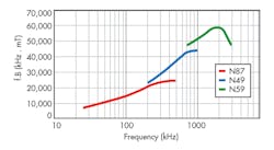
As mentioned earlier, high-speed (i.e., high switching frequency) power conversion creates an opportunity to shrink magnetic circuit elements (transformers, inductors). Here, designs are selected based on switching frequency, topology (current waveforms), and voltage step-down ratio (turns). Many options are available for 50- to 500-kHz operation. In addition, recent introductions3 by TDK (N59) and Hitachi Metals (ML91S), which are optimized for 1 to 2 MHz, open up new opportunities for circuit designers to choose new high-frequency ferrite materials (Fig. 5).
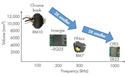
As shown in Fig. 6, size is reduced and transformer format changes (from bobbin-based to planar) with increases in frequency. The change to soft-switching topology and use of high-performance GaN also increases efficiency, thus helping to minimize heatsinking, too.
This higher power density (W/in.3) translates into smaller power converters or more power in the same size case. For consumers, this means a single, small, light travel adapter that can more quickly charge a laptop, a tablet, a smartphone and low-power wearable devices.
Recent efficiency certification requirements4, such as the U.S. Department of Energy’s “Level VI” and the European Union’s “Certificate of Conformance” (CoC), plus connector/interfacing standards like USB-PD5, have introduced higher performance demands from, and pushed more components into, power-supply designs. Without an improvement in power-conversion density enabled by higher switching frequency, adapters will only increase in size and cost. In non-mobile applications like flat-screen TVs, smaller size can be translated as low-profile power conversion and the elimination of the thick power-supply “bulge.”
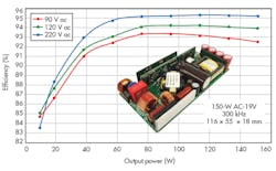
In one simple example, an AC-19V adapter was built from commercially available control ICs, and a GaN Power IC high-voltage powertrain (Fig. 7). The topology is standard critical conduction- (or boundary-) mode boost PFC (using NCP1615), followed by a ZVS LLC circuit (NCP1399AX1) and synchronous rectification (NCP43080). Note that the GaN Power ICs are mounted on a daughtercard, remote from the control ICs, indicating a robust digital connection between control IC pulse-width-modulation (PWM) output and GaN Power IC input.
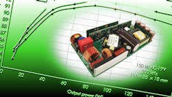
Typical switching frequencies for this type of application are 65 to 100 kHz, with power densities around 9 W/in.3. In this example, the frequency was increased to ~300 kHz (the maximum allowed by the available control ICs). With the GaN Power ICs, the “cased” power density increased to over 20 W/in.3 with commensurate efficiency increases to over 95% at 220 VAC and over 92% at 90 VAC, full load.
Keeping an Eye on Cost
As low-voltage Si CMOS manufacturing with finer geometries has moved to 200-mm or even 300-mm-diameter wafers, 650-V GaN Power ICs are manufactured on legacy, high-capacity 150-mm equipment. The ability to grow a very thin GaN epitaxial layer onto an inactive Si substrate (GaN-on-Si) has led to more cost-effective, high-volume manufacturing. And when coupled with standard QFN packaging, the GaN Power ICs have become cost-competitive at a component level. When additional functions and features, such as driver, logic, and protection, are considered, in addition to savings realized with magnetics, PCB, case, heatsinks, etc. due to higher frequency and higher efficiency, it’s possible to reduce overall system bill-of-material (BOM) costs.
As frequencies increase, the transition from traditional wound bobbins to planar magnetics—where the transformer windings are the embedded PCB tracks—represents another cost-saving area. Typically, 40% of the cost of a bobbin-based component is in manual labor. With planar magnetics, cores are simply assembled by the power-supply manufacturing company. At 150 W, the cost of the transformer can drop by more than 50% from a 100 kHz design to one at 500 kHz.
For the system designer, integration means simpler, faster component selection and layout, more predictable prototypes with easier qualification, and shorter times to market. For the purchasing managers and quality engineers, integration means fewer components to select, qualify, and procure, thus reducing time and cost associated with those tasks.
To summarize, GaN Power ICs offer one way to achieve predictable, high-performance, commercially-viable power converters. Their integrated building blocks enable fast-switching topologies with simple “digital-in, power-out” performance. When switching frequencies increase from 100 kHz to 300 kHz on up to 1 MHz, power converters simultaneously achieve size reductions and increased efficiencies.
References:
1. ““Breaking Speed Limits with GaN Power ICs,” D. Kinzer, APEC 2016 keynote, http://www.navitassemi.com/white-papers-articles/
2. “650V AllGaN™ Power IC for Power Supply Applications,” M. Giandalia, WiPDA 2016, http://www.navitassemi.com/white-papers-articles/
3. TDK/EPCOS N59/PC200: https://en.tdk.eu/tdk-en/374108/tech-library/articles/products---technologies/products---technologies/low-losses-at-high-frequencies/1206400
Hitachi Metals ML91S: http://www.hitachi-metals.co.jp/e/press/news/2016/n0404.html
4. “Efficiency standards for external power supplies,” CUI
5. “USB Power Delivery,” Universal Serial Bus
About the Author
Voice Your Opinion!
To join the conversation, and become an exclusive member of Electronic Design, create an account today!

Leaders relevant to this article:
