IC Takes Major Step Closer to Zero-Power Digitized Temperature Sensor

The challenge facing designers trying to incorporate temperature sensing into an IoT application, especially if it’s a medical or wearable situation, is two-fold. First, where do you get the needed long-term power—from a tiny battery or harvesting? Second, how do you efficiently digitize that analog-sensor signal?
An IC using a new sensor/digitizer architecture, developed by a team at the Energy-Efficient Microsystem Lab, University of California, San Diego, addresses this issue. They claim that its innovative design, which consumes a little over 100 picowatts, is lower than existing techniques by a factor of over 600. The resultant device greatly extends battery life or eases use of harvesting.
Patrick Mercier, an electrical engineering professor at UC San Diego Jacobs School of Engineering and the study’s senior author (also the co-director for the Center for Wearable Sensors at UC San Diego), says “Our new near-zero-power technology could one day eliminate the need to ever change or recharge a battery.”
1. This near-zero-power temperature sensor/digitizer, which consumes just on 113 picowatts of power, was fabricated in a standard 65-nm CMOS process and has a die size of 0.15 mm2.
The sensor/converter uses a standard 65-nm process and has an area of 0.15 mm2 (Fig. 1). It operates from −20°C to +40°C, which is wide enough for the target applications, while its one-second update rate is also adequate for most temperature-related situations.
Gate Leakage is a Good Thing?
The design involves two major functional blocks: a pair of current sources and a temperature-to-digital readout. Key to the design is leveraging the gate-leakage effects in transistors for an ultra-low-power current source.
As the gate material of a transistor becomes thinner, this material is no longer able to fully block electrons from leaking through as it can in a larger-geometry device, a phenomenon called the quantum-tunneling effect. The UCSD design takes this gate leakage—normally considered a problem—and uses the associated tiny electron flow to build a current source. This current source is then utilized to create a lower-power approach to digitization.
Note that one common way to digitize temperature (or other sensor output currents) is to pass the current though a temperature-dependent resistor, and then convert the resultant voltage across the resistor. However, that’s a power-hungry approach, so the team instead decided to digitize the temperature directly with a variation on the dual-slope analog-to-digital conversion technique.
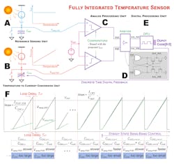
2. Architecture of the proposed temperature sensor: A temperature-stable current source was employed to generate a constant-with-temperature (CWT) ramp voltage, Vramp , CWT , by charging capacitor CREF (A). A proportional-to-absolute temperature (PTAT) current source, which was employed as the temperature sensing core by converting temperature to a corresponding current, generated a PTAT ramp voltage, Vramp, PTAT , by charging a digitally-controllable bank of capacitors CDAC (B). An analog processing unit consisting of a temperature-stabilized VRG, comparators, and an arbiter was implemented to translate the temperature-encoded analog voltages to digital signals (C). Schematic of the Arbiter (D). A digital processing unit (DPU) processes the information, controls CDAC , and generates the digital codes corresponding to the ambient temperature (E). An example operation of the DPU illustrates that CDAC was tuned via discrete-time digital feedback to match the rising time of Vramp, CWT in the reference sensing unit (RSU) (F).
They built two current sources—one to charge a capacitor for a fixed amount of time independent of the temperature, and the other with a charging rate that’s a function of temperature (Fig. 2). As the temperature changes, the design adapts so that the temperature-dependent current source charges in the same amount of time as the fixed current source.
This is accomplished via a digital feedback loop, which equalizes the charging times by connecting the temperature-dependent source to capacitors of different sizes, with the size of the capacitor directly proportional to the temperature being assessed. As the temperature falls, the temperature-dependent source will charge more slowly. Therefore, the feedback loop adjusts by switching in a smaller capacitor, which in turn points to a specific readout value.
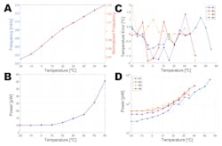
3. Depicted are the experimental results of the intrinsic oscillator and temperature sensor: Measured oscillation frequency of the intrinsic oscillator across temperature at VDD = 0.5 V (A). Measured power of the intrinsic oscillator across temperature at VDD = 0.5 V (B). Measured temperature error across temperature at VDD = 0.5 V (C). Measured power of the temperature sensor across temperature at VDD = 0.5 V (D).
Accuracy was on the order of ±1°C (Fig. 3C), while power consumption was a little over 100 pW, rising with temperature (Fig. 3D). The complete, detailed technical paper, “Near-Zero-Power Temperature Sensing via Tunneling Currents Through Complementary Metal-Oxide-Semiconductor Transistors,” is available online at Nature Scientific Reports, complete with schematics, equations, operating principles, analysis, graphs, and performance results.

About the Author

Bill Schweber
Contributing Editor
Bill Schweber is an electronics engineer who has written three textbooks on electronic communications systems, as well as hundreds of technical articles, opinion columns, and product features. In past roles, he worked as a technical website manager for multiple topic-specific sites for EE Times, as well as both the Executive Editor and Analog Editor at EDN.
At Analog Devices Inc., Bill was in marketing communications (public relations). As a result, he has been on both sides of the technical PR function, presenting company products, stories, and messages to the media and also as the recipient of these.
Prior to the MarCom role at Analog, Bill was associate editor of their respected technical journal and worked in their product marketing and applications engineering groups. Before those roles, he was at Instron Corp., doing hands-on analog- and power-circuit design and systems integration for materials-testing machine controls.
Bill has an MSEE (Univ. of Mass) and BSEE (Columbia Univ.), is a Registered Professional Engineer, and holds an Advanced Class amateur radio license. He has also planned, written, and presented online courses on a variety of engineering topics, including MOSFET basics, ADC selection, and driving LEDs.
Comment About the Article
To join the conversation, and become an exclusive member of Electronic Design, create an account today!

Leaders relevant to this article: