Do More with Less: Designing With Power-Efficient Data Converters
Download this article in PDF format.
No matter your target application, it’s desirable to make the design as “green” as possible in today’s world. That means meeting the required performance goals with the minimum power consumption.
In data-acquisition design, an analog-to-digital converter (ADC) is available for just about every application. However, there can be considerable overlap, and high performance, low power consumption, and small size are often conflicting goals.
For example, higher-performance converter architectures tend to require more silicon and consume more power, which leads to larger packages. Prioritizing low power consumption and small size may require compromising the performance, perhaps reducing the resolution or sample rate.
The power consumption of the data-acquisition signal chain also depends heavily on two additional factors: the power dissipated by the input driver and the efficiency of the power supply. This can be challenging for systems that require a combination of high performance and low power.
Let’s look at some power-efficient data-acquisition designs targeting three very different applications and performance levels, and examine what steps we can take to reduce power consumption while maintaining performance.
Sponsored Resources:
- Low-Power Sensor Measurements: 3.3V, 1ksps, 12-bit Single-Ended, Dual Supply
- Using interleaving with SAR ADCs for lower power, smaller size and lower cost
- Designing a modern power supply for RF sampling converters
Low-Speed Applications
Many data-acquisition applications don't need blazing speeds because the physical quantities measured by the input sensors change relatively slowly. In this application space, battery-powered designs are common.
Examples of such systems include wearables (fitness bands, smart watches; CO2 detectors, smoke detectors, or smart thermostats in home automation); industrial modules (remote sensors or data loggers; glucose meters, cardiac monitors, and similar portable or implantable medical devices); and security equipment (cameras or motion detectors).
These systems often must run for extended periods—months or even years—on a single battery charge. To minimize power consumption, each electronic component in the design should consume as little power as possible when performing its necessary function and go into a low power state as often as possible. Reducing the power consumption translates into extended battery life and a market advantage.
Many low-power systems must also be very small. The size constraint might limit the number of suitable devices, and potentially force the selection of a converter with higher power consumption or lower performance than desired.
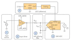
Figure 1 shows the main building blocks in a low-power data-acquisition system. The characteristics of the input source (1)—output impedance, output voltage, frequency, etc.—determine the selection of the input driver (2) and the anti-aliasing filter (3). The driver output feeds the SAR ADC (4); the SAR power consumption scales with the sample rate. The LDO (5) provides low-noise system power and the voltage reference for the ADC.
1. A low-power data-acquisition node includes five main blocks. (Source: TI “Three 12-Bit Data Acquisition Reference Designs Optimized for Low Power and Ultra-Small Form Factor” PDF, p. 5)
Let’s examine three separate designs optimized for three different sets of requirements. All three are based on the TI ADS7042, a 12-bit SAR converter optimized for extremely low-power, small-form-factor applications. The examples show some of the design tradeoffs needed to give the lowest power and smallest size for the given applications.
Design number 1 is a 12-bit, 500-ksample/s data-acquisition system optimized for applications such as current monitoring, battery monitoring, electromyography or EMG, skin impedance, and wearable fitness devices. If the input signal has a high-impedance output and low input frequency, it’s important to isolate the ADC input by adding a low-power input driver. The device chosen is the OPA314, a low-power, low-noise op amp with rail-to-rail inputs and outputs (RRI/O) and a gain bandwidth (GBW) of 3 MHz. The device provides the output current drive needed to charge the internal switched-capacitor input of the SAR ADC. This design optimizes the drive amplifier and anti-aliasing filter for the required sampling rate and consumes 1 mW of power.
Design number 2 optimizes the drive amplifier and anti-aliasing filter for an application with a sampling rate up to 1 Msample/s. For example, a use case may have an input signal that’s greater than 10 kHz and requires a response time of less than 2 µs. Compared to the previous design, this design uses an OPA835 for the input driver. With a unity-gain bandwidth of 56 MHz, this higher-bandwidth amplifier still satisfies the power requirements and ENOB for the application. This design consumes 2.5 mW of power.
Design number 3 suits low-sample-rate (<1 ksample/s) applications such as tilt, gyro, pressure, temperature, gas, chemical, or blood-glucose sensor measurements. The critical parameter in these cases is the output impedance of the input source. If the input is very slow moving, has a low output impedance, and the overall system ENOB isn’t a critical parameter, it’s possible to completely omit the input driver.
Figure 2 compares features and power consumption of the three designs.
2. These represent three design options for a low-power data-acquisition system. (Source: TI “Three 12-Bit Data Acquisition Reference Designs Optimized for Low Power and Ultra-Small Form Factor” PDF, p. 2)
TI’s TIPD168 is a verified Precision Reference Design that covers the three designs discussed. The package includes a detailed description of the design procedure, simulated results, and the actual test results of a discrete data-acquisition block.
Power-Efficient Data Converters for High-Performance Applications
What if your application requires higher converter performance than we’ve talked about thus far, but low power is still a requirement? The pipeline converter is the first option considered by many designers. It offers a high sample rate, but is a power hog because it requires a greater number of internal comparators and amplifiers than a successive-approximation converter of the same resolution.
Combining the output of multiple converters—a technique known as interleaving—enables a system to maintain resolution while increasing the effective sample rate, helping to bridge the speed gap between SAR and pipeline architectures. In an equivalent system, interleaved SAR ADCs can help reduce the overall power consumption, cost, and size of the design compared to pipeline ADCs.
An interleaved converter samples the input signal with multiple synchronized data converters running from a common clock with multiple phases. The sampling period for each converter is phase-shifted, and the results from each converter are then combined to form the output data stream, effectively increasing the system sampling rate while maintaining the resolution of the individual ADCs.
Phase-shifted versions of a single clock generate the conversion signals for all of the ADCs. The phase shift between clocks for an n-converter design is (360/n)°. Therefore, in a three-converter design, the clocks should be phased at intervals of 120°.
Pay Attention to ADC Differences
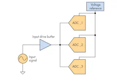
Interleaving multiple ADCs may have advantages in power efficiency, but even with modern production techniques, the ADCs aren’t completely identical, and this must be taken into account. For example, mismatches between external voltage references and driver amplifiers are potential sources of error. A single front-end driver amplifier for all ADCs eliminates these offset variations, and a single voltage reference eliminates input signal gain variations. Figure 3 shows the resulting block diagram.
3. A single input buffer and voltage reference eliminate two error sources in an interleaved converter design. (Source: TI “Using interleaving with SAR ADCs for lower power, smaller size, and lower cost” PDF, p. 2)
It’s important to calibrate out mismatches in offset and gain errors between the individual ADCs to achieve the highest performance from the interleaved design. Otherwise, the offset error will appear as a noise spur at the sampling frequency of the ADC, and the gain error will appear as a noise spur at the sampling frequency plus or minus the input signal frequency. These errors will degrade the ADC’s overall performance, reducing the signal to-noise ratio (SNR).
These errors can be calibrated out with post-processing, but this causes additional complexity for the host microcontroller. To eliminate this additional complexity, some SAR ADCs offer extremely low gain error and integrated offset-calibration circuitry.
TI’s ADS7056, for example, is a SAR ADC with an integrated offset-calibration feature and a typical gain error of only ±0.01% (or 3.2 LSBs at 14 bits). As a result, the ADS7056 doesn’t generally require gain-error calibration.
4. Interleaving three ADS7056 SAR converters gives three times the sampling rate with only a slight degradation in SNR and THD. (Source: TI “Using interleaving with SAR ADCs for lower power, smaller size, and lower cost” PDF, p. 3, Table 1)
In a performance comparison, three 14-bit ADS7056 SAR ADCs with a sampling rate of 2.5 Msamples/s each were interleaved to achieve an effective system sampling rate of 7.5 Msamples/s. Figure 4 compares the interleaved system performance compared to that of an individual ADC. The overall performance metrics of the ADC—including resolution, SNR, and total harmonic distortion (THD)—remain almost the same, but the sampling rate increases by a factor of three.
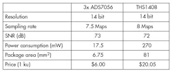
How does the performance of an interleaved SAR design compare to that of a pipeline converter with equivalent performance? Figure 5 tells the tale. The resolution, sampling rate, and SNR are comparable, while the power, package size, and price are greatly reduced. The improvement in power consumption is particularly striking—a reduction of more than 93%!
5. The chart compares the performance of an interleaved SAR design versus a pipeline design. (Source: TI “Using interleaving with SAR ADCs for lower power, smaller size, and lower cost” PDF, p. 3, Table 2)
At High Sample Rates, Take a System-Level Approach to Lowering Power Consumption
When dealing with gigabit-per-second sample rates, a low-power SAR architecture isn’t an option, so we must cast our net a little wider. One valuable power-reduction technique is to pick an ADC that allows you to eliminate other devices for lower overall system power consumption, although the ADC itself might not be the lowest-power component available with the required performance.
The ADC32RF45 is a good example. It’s a dual-channel, 14-bit, 3-Gb/s ADC for high-performance RF applications such as military radios, LAN/WAN test equipment, and signal analyzers. These applications aren’t usually considered low power, but the ADC32RF45’s high sample rate makes it possible to eliminate the entire RF downconversion stage. The result is a simpler signal chain with a much smaller footprint on the printed circuit board (PCB).
The power supply presents another opportunity to reduce power consumption. The traditional power supply for a high-current converter starts with a switching dc-dc converter. A switcher is an efficient means to generate the required voltage, but the output includes switching noise and flicker noise. Consequently, an LDO regulator is added to improve the power-supply noise rejection, followed by a power-supply filter. Capacitors at the ADC pins provide bypassing of the converter switching currents.
A modern dc-dc regulator such as TPS62085 uses a switching frequency of 2.4 MHz to reduce inductor size. At this frequency, though, the power-supply rejection ratio (PSRR) of the LDO may only be 20 to 30 dB. It’s possible to eliminate the LDO and achieve a similar level of attenuation with an optimized power-supply filter that’s tuned to provide 20 to 30 dB at the TPS60285’s switching frequency.
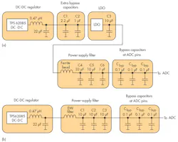
6. The traditional power supply design (a) includes an LDO to remove switching noise. Optimizing the power-supply filter (b) allows its elimination. (Source: TI “Designing a modern power supply for RF sampling converters” PDF, Figs. 2 and 4)
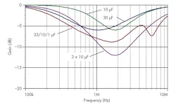
Figure 6 shows the traditional and improved power-supply designs. The power-supply filter in the traditional version has several different capacitors to try and filter a wide range of spur frequencies. The tuned filter uses three parallel 10-µF capacitors to achieve a 6-dB performance improvement at 2 MHz. Figure 7 compares the responses of the two capacitor combinations, plus the single-capacitor responses.
7. A simulation shows the improved response of the 10-µF parallel capacitor combination versus the 33-µF/10-µF/1-µF combination, including package parasitics. (Source: TI “Designing a modern power supply for RF sampling converters” PDF, Fig. 3)
The optimized design also replaces the ferrite bead with an electromagnetic-interference (EMI) suppression filter. To be effective against switching noise, the ferrite bead should have a high impedance at the 2-MHz frequency of interest. Most ferrite beads have high impedance around 100 MHz, but very little impedance at low frequencies, so they’re not effective at attenuating switching spurs. An EMI suppression filter such as Murata’s NFM31PC276B0J3 has an insertion loss of approximately 85 dB at 3 MHz and can provide as much as 25 dB of rejection in the application.
Read more about power supply design for high-speed data converters in this article from TI’s Analog Applications Journal. For more information on Texas Instruments’ deep portfolio of ADCs, check out this product overview.
Sponsored Resources:
About the Author
Paul Pickering
Paul Pickering has over 35 years of engineering and marketing experience, including stints in automotive electronics, precision analog, power semiconductors, flight simulation and robotics. Originally from the North-East of England, he has lived and worked in Europe, the US, and Japan. He has a B.Sc. (Hons) in Physics & Electronics from Royal Holloway College, University of London, and has done graduate work at Tulsa University. In his spare time, he plays and teaches the guitar in the Phoenix, Ariz. area
Voice Your Opinion!
To join the conversation, and become an exclusive member of Electronic Design, create an account today!

Leaders relevant to this article:

